
Programming instructions

Transistors
Multisim Component Reference Guide 4-18 ni.com
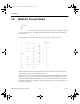
V
GS(off)
= gate-source cutoff voltage, in volts
I
S
= saturation current for the gate-drain and gate-source diode junctions
I
D
= drain-to-source current, in amperes
I
DSS
= drain-to-source saturation current, in amperes
β
= = transconductance parameter in A/V
2
l = channel-length modulation parameter measured in 1/V
Other symbols used in these equations are defined in “JFET Model Parameters and Defaults”.
Note β is not to be confused with g
m
, the AC small-signal gain mentioned later in this
chapter.
The charge storage occurring in the two gate junctions is modeled by the diode time-domain
model described in the Diodes Parts Bin chapter.
The diodes used to model the JFETs are represented by their small-signal models.
where
g
GS
and g
GD
are normally very small because the diode junctions are not forward-biased.
I
GS
and I
GD
are the diode current expressions mentioned in the diode modeling section.
g
m
= AC small-signal gain
g
DS
= small-signal forward admittance or transconductance
[]
I
V
DSS
GS off
()
2
g
dI
dV
g
dI
dV
g
dI
dV
g
dI
dV
m
D
GS
OP
DS
D
DS
OP
GS
GS
GS
OP
GD
GD
GD
OP
=
=
=
=
ComponentRef.book Page 18 Thursday, December 7, 2006 10:12 AM