
Programming instructions


Diode
National Instruments Corporation 3-3 Multisim Component Reference Guide
3.1.3 Time-Domain Model
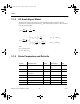
This model defines the operation of the diode, taking into account its charge-storage effects or
capacitance. There are two types of capacitances: diffusion or storage capacitance, and
depletion or junction capacitance.
The charge-storage element,
C
D
,
takes into account both of these as follows:
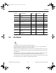
where:
C
j0
= zero-bias junction capacitance; typically 0.1 to 10 picofarads
ϕ
0
= junction potential; typically 0.5 to 0.7 volts
τ
t
= transit time; typically 1 nanosecond
m = junction grading coefficient; typically 0.33 to 0.5
and where
F
2
and
F
3
are constants whose values are:
Notes
1. The voltage drop across the diode varies depending on the set value of:
I
S
= saturation current; typically 10-14 amperes
r
S
= ohmic resistance; typically 0.05 ohms.
2. The parameter
τ
t
is proportional to the reverse recovery time of the diode. That is, it affects
the turn-off or switching speed of the diode. It is the time required for the minority carrier
to cross the junction.
3. The barrier potential for a diode is approximately 0.7 to 0.8 volts. This is not to be
confused with the model parameter
ϕ
0
given above.
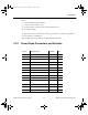
C
dI
dV
C
V
VFCj
dI
dV
C
F
F
mV
VFCj
D
t
D
D
j
D
D
t
D
D
j
D
D
=
<∗
+
≥∗
τ
ϕ
τ
ϕ
+ - for
+ for
0
-m
0
00
0
2
30
1
FFC
FFCm
m
2
1
3
1
11
=−
=− +
+
()
()
ComponentRef.book Page 3 Thursday, December 7, 2006 10:12 AM