
Service manual


35
32JW-73E
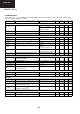
TEA1507 (IC701)
Note
1. Guaranteed by design.
Burst mode standby (pin 3)
V
th(burst)(on)
burst mode standby active threshold
voltage
at I
burst
= 6 mA 3.3 3.8 4.3 V
I
th(burst)(on)
burst mode standby active current 16 −−mA
I
th(burst)(off)
burst mode standby inactive current −−6mA
t
(burst-blank)
burst mode standby blanking time 25 30 35 µs
Valley switch (pin 8)
∆V/∆t
valley
∆V/∆t for valley recognition −85 −+85 V/µs
t
valley-swon
delay from valley recognition to switch-on − 150
(1)
− ns
Current and short winding protection (pin 5)
V
sense(max)
maximum source voltage OCP ∆V/∆t = 0.1 V/µs 0.48 0.52 0.56 V
t
propagation
delay from detecting V
sense(max)
to
switch-off
∆V/∆t = 0.5 V/µs − 140 185 ns
V
swp
short winding protection voltage 0.83 0.88 0.96 V
t
leb
blanking time for current and short
winding protection
300 370 440 ns
I
ss
soft start current V
sense
<0.5V 456075µA
Overvoltage protection (pin 4)
I
(OVP)(DEM)
OVP protection level at pin 4, set by the
demagnetization resistor R
DEM
; see
Section “OverVoltage Protection (OVP)”
54 60 66 µA
Overpower protection (pin 4)
I
(OPP)(DEM)
OPP current at pin 4, start of OPP
correction. Set by the demagnetization
resistor R
DEM
; see Section “OverPower
Protection (OPP)”
−−24 −µA
I
(OPP50%)(DEM)
OPP current at pin 4 where maximum
source voltage is limited to 0.3 V
−−100 −µA
Driver (pin 6)
I
source
source current capability of driver V
CC
= 9.5 V; V
DRIVER
=2V −−170 −88 mA
I
sink
sink current capability of driver V
CC
= 9.5 V; V
DRIVER
=2V − 300 − mA
V
CC
= 9.5 V;
V
DRIVER
= 9.5 V
400 700 − mA
V
o(driver)(max)
maximum output voltage of the driver V
CC
>12V − 11.5 12 V
Temperature protection
T
prot(max)
maximum temperature threshold 130 140 150 °C
T
prot(hyst)
hysteresis temperature − 8
(1)
−°C
SYMBOL PARAMETER CONDITIONS MIN. TYP. MAX. UNIT