
Service manual


32
32JW-73E
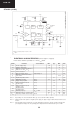
5 ELECTRICAL CHARACTERISTICS
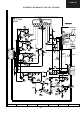
(refer to Figure 1 on page 3)
Tamb = 25°C unless otherwise specified, Vcc = ±12V, f
vert
=50Hz
Note: 1
Input voltage = 0, measured after the filter (e.g. accross the 470 nF filter capacitor)
Note: 2
Supply rejection of the positive or negative power supply. Vcc ripple =1Vpp, f=100Hz, measured on the sense
resistor.
Note: 3
Power dissipated in the circuit in the case of the application from Figure 1 and the current in the deflection
yoke adjusted to 2.5App. The corresponding power dissipated in the vertical deflection yoke is 2.8W.
Symbol Parameter Test Conditions Min. Typ. Max. Units
+Vcc Positive supply range +10 +18 V
-Vcc Negative supply range -18 -10 V
∆Vcc
Maximum recommended difference
between +Vcc and
±4V
Vcc
start
Low Vcc detection ±6.5 V
Iq Quiescent supply current Input voltage = 0 14 mA
Iy
Maximum recommended vertical
yoke current
±1.25 A
I
13
,I
12
Amplifier Input bias current -0.1
µ
A
V
OS
Output Offset voltage Note 1 -50 +50 mV
SVR Supply voltage rejection Note 2 82 dB
Fly
thr
Flyback detection threshold
(positive slope)
V(14) 1.5 V
Fly
thf
Flyback detection threshold
(negative slope)
V(14) 0.5 V
Pd
Integrated circuit
Dissipated power
Note 3 1.1 W
Fsw Switching frequency R
freq
=10kΩ 120 140 160 kHz
Fsw - op Switching frequency operative range 100 200 kHz
R
freq
Frequency controller resistor range Pin 10 7 10 14 k
Ω
Vcc–
STV9380 (IC502)
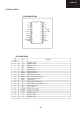
Figure 1. Test and Application Circuit
Flyback
Flyback
Output
Modulator
+
_
drive
generator
detection
+VCC
+VCC power
CFLYBACK
CFLY+
100nF
VREG
IN+
IN -
1kΩ
10kΩ
EA out
-VCC power
-VCC
-VCC
BOOT
Cboot
470nF
10kΩ
4.7nF
FREQ
FEEDCAPSGND
Pins 1,2,3,18,19,20
OUT
0.5Ω
Deflect.
Yoke*
CFLY-
+VCC
1mH
Input signal
1kΩ
220nF
-VCC
100nF
100nF 1000µF
1000µF
STV9380
100µF
14
11
9
17
560pF
150Ω
200Ω
15
16
8
TDA9380
5
6
7
4
13
12
150Ω
10
Vref
-VCC
470pF
* Deflection yoke characteristics: R = 5.5Ω, L = 7mH
100nF
Sense
resistor
f
vert
= 50Hz