
Service manual

28
32JW-73E
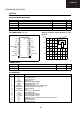
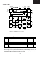
MSP3410G (IC301)
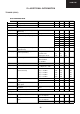
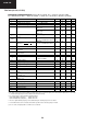
4.6.1. Absolute Maximum Ratings
Stresses beyond those listed in the “Absolute Maximum Ratings” may cause permanent damage to the device. This
is a stress rating only. Functional operation of the device at these or any other conditions beyond those indicated in
the “Recommended Operating Conditions/Characteristics” of this specification is not implied. Exposure to absolute
maximum ratings conditions for extended periods may affect device reliability.
Symbol Parameter Pin Name Min. Max. Unit
T
A
Ambient Operating Temperature − 070°C
T
S
Storage Temperature −−40 125 °C
V
SUP1
First Supply Voltage AHVSUP −0.3 9.0 V
V
SUP2
Second Supply Voltage DVSUP −0.3 6.0 V
V
SUP3
Third Supply Voltage AVSUP −0.3 6.0 V
dV
SUP23
Voltage between AVSUP
and DVSUP
AVSUP,
DVSUP
−0.5 0.5 V
P
TOT
Power Dissipation
PLCC68
PSDIP64
PSDIP52
PQFP80
PLQFP64
AHVSUP,
DVSUP,
AVSUP
1200
1300
1200
1000
960
mW
mW
mW
mW
mW
V
Idig
Input Voltage, all Digital Inputs −0.3 V
SUP2
+0.3 V
I
Idig
Input Current, all Digital Pins −−20 +20 mA
1)
V
Iana
Input Voltage, all Analog Inputs SCn_IN_s,
2)
MONO_IN
−0.3 V
SUP1
+0.3 V
I
Iana
Input Current, all Analog Inputs SCn_IN_s,
2)
MONO_IN
−5 +5mA
1)
I
Oana
Output Current, all SCART Outputs SCn_OUT_s
2) 3)
,
4) 3)
,
4)
I
Oana
Output Current, all Analog Outputs
except SCART Outputs
DACp_s
2) 3) 3)
I
Cana
Output Current, other pins
connected to capacitors
CAPL_p,
2)
AGNDC
3) 3)
1)
positive value means current flowing into the circuit
2)
“n” means “1”, “2”, “3”, or “4”, “s” means “L” or “R”, “p” means “M” or “A”
3)
The analog outputs are short-circuit proof with respect to First Supply Voltage and ground.
4)
Total chip power dissipation must not exceed absolute maximum rating.