
Service manual

26
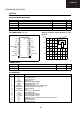
32JW-73E
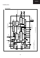
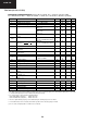
TDA7480 (IC1301,IC1302)
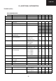
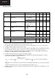
ELECTRICAL CHARACTERISTICS (Refer to the test circuit, V
CC
= ±14V; R
L
= 8Ω; R
S
= 50Ω;
R
f
= 12KΩ; Demod.. filter L = 60µH, C = 470nF; f = 1KHz; T
amb
= 25°C unless otherwise specified.)
Symbol Parameter Test Condition Min. Typ. Max. Unit
V
S
Supply Range
±
10
±
16 V
I
q
Total Quiescent Current R
L
=
∞
; NO LC Filter 25 40 mA
V
OS
Output Offset Voltage Play Condition –50 +50 mV
P
O
Output Power THD = 10%
THD = 1%
8.5
6
10
7
W
W
R
L
= 4
Ω
V
CC
=
±
10.5V
THD = 10%
THD = 1%
10
7
W
W
P
d
(*) Dissipated Power at 1W Output
Power
R
f
= 12K
Ω
P
Ο
= 1W 1 W
P
DMAX
Maximum Dissipated Power P
Ο
= 10W THD 10%
R
th-j-amb
= 38°C/W (Area 12cm
2
)
1.8 W
η
Efficiency
≡
P
O
P
O
+
P
D
≡
P
O
P
I
(**)
THD 10%
R
th-j-amb
= 38°C/W (Area 12cm
2
)
80 85 %
THD Total Harmonic Distortion R
L
= 8
Ω
; P
O
= 0.5W 0.1 %
I
max
Overcurrent Protection
Threshold
R
L
= 0 3.5 5 A
T
j
Thermal Shut-down Junction
Temperature
150 °C
G
V
Closed Loop Gain 29 30 31 dB
e
N
Total Input Noise A Curve
f = 20Hz to 22KHz
7
12
µ
V
µ
V
R
i
Input Resistance 20 30 K
Ω
SVR Supply Voltage Rejection f = 100Hz; V
r
= 0.5 46 60 dB
T
r
, T
f
Rising and Falling Time 50 ns
R
DSON
Power Transistor on Resistance 0.4
Ω
F
SW
Switching Frequency 100 120 140 KHz
F
SW_OP
Switching Frequency Operative
Range
100 200 KHz
B
F
Zero Signal Frequency
Constant (***)
1.4x10
9
Hz
Ω
R
F
Frequency Controller Resistor
Range (****)
71214K
Ω
MUTE & STAND-BY FUNCTIONS
V
ST-BY
Stand-by range 0.8 V
V
MUTE
Mute Range 1.8 2.5 V
V
PLAY
Play Range (1) 4 V
A
MUTE
Mute Attenuation 60 80 dB
I
qST-BY
Quiescent Current @ Stand-by 3 5 mA
*: The output average power when the amplifier is playing music can be considered roughly 1/10 of the maximum output power. So it is useful
to consider the dissipated power in this condition for thermal dimensioning.
**: P
O
= measured across the load using the following inductor:
COIL 58120 MPPA2 (magnetics) TURNS: 28
∅
1mm
COIL77120 KOOL M
µ
(magnetics) TURNS: 28
∅
1mm
***: The zero-signal switching frequency can be obtained using the following expression: F
SW
= B
F
/R
F
****: The maximum value of R
F
is related to the maximum possible value for the voltage drop on R
F
itself.
(1): For V
12
>5.2V, an input impedance of 10K
Ω
is to be considered.