
Users Manual
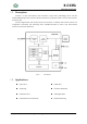
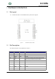
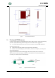
Table Of Contents
- 1 Module Overview
- 1.1 Features
- 1.2 Description
- 1.3 Applications
- CONTENTS
- LIST OF FIGURES
- HISTORY
- 2 Hardware Introduction
- 2.1 Pin Layout
- 2.2 Pin Description
- 2.3 Physical Dimensions
- 2.4 On-board Chip Antenna
- 2.5 Ordering Information
- 3 Electrical Characteristics
- 3.1 Absolute Maximum Ratings
- 3.2 Recommended Operating Conditions
- 3.3 ESD
- 3.4 WiFi/BLE RF Standards
- 4 Peripheral Schematics
- 5 Product Handling
- 5.1 Reflow Profile
- 5.2 Storage Conditions
- 5.3 Device Handling Instruction (Module IC SMT Prepara
- 6 Contact Information

X-C13SL
802.11bgn and BLE SoC
Shanghai ChipFresh Internet of Things Technology Co., Ltd
8
2 Hardware Introduction
2.1
Pin Layout
X-C13SL comes with a on-board PCB antenna, please refer to Figure 2.
Figure 2. X-C13SL Pin Layout (Top View)
2.2 Pin Description
The module has 34 pins. See pin definitions in Table 1.
Pin
Describtion
Type
Function
1,17,18,34
Ground
P
GND
2,3,4,5,6
-
-
-
7
GPIO1
IPU/O
SPI,PWM
8
GPIO20
IPU/O
SPI,PWM
9,20
+3.3V
3V3
P
The maximum output current of the external power
supply is recommended to be above 500mA.
10
GPIO7, FSPID, MTDO
11
GPIO21
IPU/O
SPI,PWM
12
GPIO22
IPU/O
SPI,PWM
13
GPIO0
IPU/O
SPI,PWM
14
N,C