
User's Manual
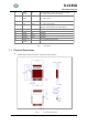
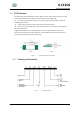
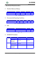
Table Of Contents

X-C13SG
802.11bgn and BLE SoC
Shanghai ChipFresh Internet of Things Technology Co., Ltd
7
2 Hardware Introduction
2.1
Pin Layout
X-C13SG comes with a on-board PCB antenna, please refer to Figure 2.
Figure 2. X-C13SG Pin Layout (Top View)
2.2
Pin Description
The module has 23 pins. See pin definitions in Table 1.
Pin Describtion Type Function
1,8,14,16,23 Ground P GND
2 GPIO8 IPD
Internal 10K pull-down resistor,
Boot select:
Low: boot from module flash.
High: boot from external UART.
This is used for factory firmware program, leave it
unconnected for user application
3 RESET I,PU “Low” effective reset input.
4
UART1_RX
GPIO11 I
3.3V TTL UART1 Debug Input
SPI, PWM
5 GPIO14 IPU/O SPI, DAC, ADC
6 UART0_RX
GPIO7
I 3.3V TTL UART0 Communication Input
7 UART0_TX
GPIO16
O,PU 3.3V TTL UART0 Communication Output
9 GPIO12 I/O SPI, PWM. ADC
10 GPIO1 IPU/O SPI,PWM