
User's Manual

SIM900E Document
- 11 -
DCS1800 1805 ~ 1880MHz 1710 ~ 1785MHz
PCS1900 1930 ~ 1990MHz 1850 ~ 1910MHz
5. RF Circuit Routing Constraints
5.1. General recommendations
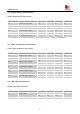
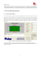
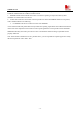
To route the RF antenna signals, the following recommendations must be observed for PCB layout: The RF
signals must be routed using traces with a 50 characteristic impedance. Basicaly, the characteristic impedance
depends on the dielectric constant (εr) of the material used, trace width (W), trace thickness (T), and height (H)
between the trace and the reference ground plane. In order to respect this constraint, SIMCom recommends that a
MicroStrip structure be used and trace width be computed with a simulation tool (such as CITS25, shown in the
figure below)
Figure 5: CITS25 screenshot for MicroStrip design power mode diagram
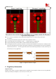
The trace width should be wide enough to maintain reasonable insertion loss and manufacturing reliability.
Cutting out inner layers of ground under the trace will increase the effective substrate height; therefore, increasing
the width of the RF trace.