
User's Manual

Smart Machine Smart Decision
SIM5360A_User_Manual_V1.03 2014-07-03
56
● GSM850<0.5dB
● PCS1900 <0.9dB
● WCDMA 1900<0.9dB
● WCDMA 850<0.5dB
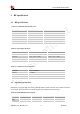
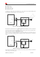
To facilitate the antenna tuning and certification test, a RF connector and an antenna matching circuit
should be added. The following figure is the recommended circuit.
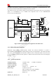
R2
C1
60
MODULE
59
MAIN_ANT
GND
C2
58
GND
R1
Antenna feed pad
Matching circuit
J1
Figure 39: Antenna matching circuit (MAIN_ANT)
In this figure, the components R1,C1,C2 and R2 is used for antenna matching, the value of components
can only be got after the antenna tuning, usually, they are provided by antenna vendor. By default, the R1,
R2 are 0 ohm resistors, and the C1, C2 are reserved for tuning.
The RF test connector in the figure is used for the conducted RF performance test, and should be placed as
close as to the module’s antenna pin. The traces impedance between components must be controlled in
50ohm.
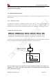
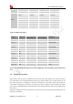
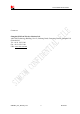
R5
C3
MODULE
82
DIV_ANT
GND
C5
58
R3
Antenna feed pad
Matching circuit
J3
Figure 40: Antenna matching circuit (DIV_ANT)
In above figure, the components R3,C3,C5 and R5 is used for diversity antenna matching. The method of
antenna tuning is same as MAIN_ANT.