
User's Manual

SHANGHAI SIMCOM LIMITED
17
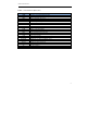
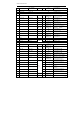
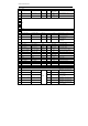
9
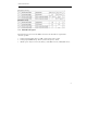
GPIO_93 OTG_EN GPIO_93 P3
DO;
BB-PD:nppukp
Configurable I/O
10
GPIO_94 ALSP_INT_N
GPIO_94*
P3
DI;
BB-PD:nppukp
Configurable I/O
11
GPIO_95 CHG_EN
GPIO_95*
P3
DO;
BB-PD:nppukp
Configurable I/O
12
GPIO_96 VBUS_OTG_EN
GPIO_96*
P3
DO;
BB-PD:nppukp
Configurable I/O
13
GPIO_97 NFC_DWL_REQ
GPIO_97*
P3
DI;
B-PD:nppukp
Configurable I/O
14
GPIO_110 NFC_INT_N
GPIO_110*
P3
DI;
B-PD:nppukp
Configurable I/O
15
GPIO_65 MAG_RESET
GPIO_65*
P3
DI;
B-PD:nppukp
Configurable I/O
16
GND
17
GND
18
GND
19
GND
20
GND
21
GND
22
GND
23
GND
24
GND
25
GND
26
GND
27
GND
28
GND
29
GND
30
GND
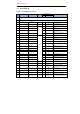
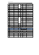
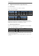
NOTE:I/O parameter definitions
Symbol
*
General purpose wakeup
AI Analog input
AO Analog output
B Bidirectional digital with CMOS input
CSI Supply voltage for MIPI_CSI circuits and I/Os; tied to VDD_MIPI_CSI (1.8 V only)
DI Digital input(CMOS)
DO Digital output(CMOS)
DSI Supply voltage for MIPI_DSI I/Os; tied to VDD_QFPROM_PRG (1.8 V only)
H High-voltage tolerant
KP Contains an internal weak keeper device (keepers cannot drive external buses)
NP Contains no internal pull
PD Contains an internal pulldown device
PU Contains an internal pullup device
PI Power input
PO Power output
V_G
Selectable supply for GPIO circuits; options include:
VIN0: 3.6 V VIN1: 3.075 V
VIN2: 1.2 V VIN3: 1.8 V
V_INT Internally generated voltage supply voltage for some power on circuits
Z High-impedance (high-Z) output