
User's Manual
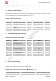
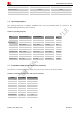
Table Of Contents
- Contents
- Version History
- 1 Introduction
- 2 Key features
- 3 Terminal dimensions
- 4 Installation
- 5 Interface introduction
- 6 Application Interface
- 7 Electrical, Reliability and Radio Characteristics
- 8 Software/ Firmware Upgrade
- Appendix

Smart Machine Smart Decision
T5320+G_User Guide_V1.01 29 2013-04-15
7 Electrical, Reliability and Radio Characteristics
7.1 Absolute Maximum Ratings
The absolute maximum ratings stated in following table are stress ratings under non-operating conditions. Stresses
beyond any of these limits will cause permanent damage to T5320+G.
Table 18: Absolute maximum ratings
Symbol Parameter Min Typ Max Unit
VBAT Power supply voltage 5 - 30 V
V
I
*
Input voltage -0.3 - 2.8 V
I
I
*
Input current - - 6 mA
I
O
*
Output current - - 6 mA
*
These parameters are for digital interface pins, such as GPIO, UART.
7.2 Recommended Operating Conditions
Table 19: Recommended operating conditions
Symbol Parameter Min Typ Max Unit
VBAT Power supply voltage 5 5 30 V
I
IH
High-level input current -10 - 10 uA
I
IL
Low-level input current -10 - 10 uA
V
IH
High-level input voltage 2.4 - - V
V
IL
Low-level input voltage - - 0.4 V
V
OH
High-level output voltage 2.6 - - V
V
OL
Low-level output voltage - - 0.1 V
T
OPER
Operating temperature -35 +25 +80 ℃
T
STG
Storage temperature -40 +85 ℃
7.3 Electro-Static Discharge
T5320+G is an ESD sensitive component, so more attention should be paid to the procedure of handling and
packaging. The ESD test results are shown in the following table.
Table 20: The ESD characteristics (Temperature: 25 , Humidity℃ : 45 %)
Pin Contact discharge Air discharge
Shell ±10KV ±15KV