
User's Manual

SIM908 Document
- 7 -
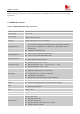
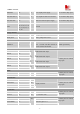
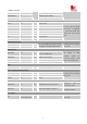
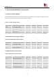
GPIO4/KBC0 34 GPIO4/keypad column 0
GPIO5/KBC1 35 GPIO5/keypad column 1
GPIO6/KBC2 36 GPIO6/keypad column 3
Serial port
RXD 68 I Receive data
TXD 71 O Transmit data
RTS 66 O Request to send
CTS 67 I Clear to send
DCD 70 O Data carrier detect
RI 69 O Ring indicator
DTR 72 I Data terminal ready
If only TXD and RXD
are used, it is suggested
to pull down DTR, and
others pins can be kept
open.
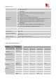
GPS/Debug interface
GPS/DBG-TXD 15 O
GPS/DBG-RXD 16 I
For GPS NMEA information output ,
debugging and upgrading firmware
If these pins are unused,
keep open.
SIM interface
SIM-VDD 20 O
Voltage supply for SIM card. Support
1.8V or 3V SIM card
SIM-DATA 17 I/O SIM data input/output
SIM-CLK 19 O SIM clock
SIM-RST 18 O SIM reset
All signals of SIM
interface should be
protected against ESD
with a TVS diode array.
ADC
ADC 47 I Input voltage range: 0V ~ 2.8V If it is unused, keep open.
Pulse width modulation( PWM )
PWM1 48 O PWM
PWM2 49 O PWM
PWM3 50 O PWM
If these pins are unused,
keep open.
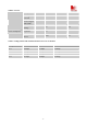
GSM/GPS RF interface
GSM-ANT 59 I/O GSM radio antenna connection
Impendence must be
controlled to 50Ω.
GPS-ANT 79 I GPS radio antenna connection
Impendence must be
controlled to 50Ω.
Not connect
NC
4,11,12,13,29,30,
38,39,45,46,53,54
-
These pins should be
kept open.