
User's Manual
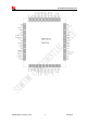
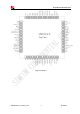
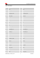
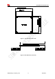
Table Of Contents
- RevisionHistory
- Introduction
- PackageInformation
- ApplicationInterfaceSpecification
- RFSpecification
- ReliabilityandOperatingCharacteristics
- GuideforProduction
- Appendix

Smart Machine Smart Decision
SIM5320ALD_User Manual_V1.01 2014-08-20
19
PCM_SYNC/GPIO2 I
General Input PIN. It also can be
multiplexed as the PCM_SYNC pin.
PCM_CLK/GPIO3 O
General Output PIN. It also can be
multiplexed as the PCM_CLK pin.
PCM_DOUT/GPIO5 O
General Output PIN. It also can be
multiplexed as the PCM_DOUT pin.
GPIOs
GPIO1 O
Output PIN as LED control for
network status.
If it is unused, keep open.
GPIO4 I Input PIN as RF operating control.
GPIO40 O
Output PIN as operating status
indicating of module.
GPIO41 I/O
General input/output PIN. It can be
used as wake/interrupt signal to host
from module
GPIO43 I/O
General input/output PIN. It can be
used as wake/interrupt signal to
module from host.
GPIO44 I/O General input/output PIN.
GPIO42 I/O General input/output PIN.
Other interface
RESET I System reset in, active low.
CURRENT_SINK I
Current source of ground-referenced
current sink
Refer to 3.13.1
ADC1 I Analog Digital Converter Input
Refer to 3.13.3
ADC2 I Battery temperature ADC input pin
MAIN_ANT I/O ANT soldering pad
2.3 Package Dimensions
The following figure shows mechanical dimensions of SIM5320ALD.