
User's Manual

Smart Machine Smart Decision
SIM5320_Hardware Design_V1.01 2011-11-10
44
4.3 Antenna Design Guide
SIM5320AD provides RF antenna interface. Customer’s antenna should be located in the host board and
connected to module’s antenna pad through micro-strip line or other types of RF trace and the trace
impedance must be controlled in 50Ω. SIMCom recommends that the total insertion loss between the
antenna pad and antenna should meet the following requirements:
● GSM900/GSM850<0.5dB
● DCS1800/PCS1900 <0.9dB
● WCDMA 1900<0.9dB
● WCDMA 850<0.5dB
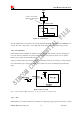
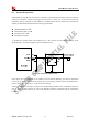
To facilitate the antenna tuning and certification test, a RF connector and an antenna matching circuit
should be added. The following figure is the recommended circuit.
Figure 32: Antenna matching circuit
In this figure, the components R1,C1,C2 and R2 is used for antenna matching, the value of components
can only be got after the antenna tuning, usually, they are provided by antenna vendor. By default, the R1,
R2 are 0 ohm resistors, and the C1, C2 are reserved for tuning.
The RF test connector in the figure is used for the conducted RF performance test, and should be placed as
close as to the module’s antenna pin. The traces impedance between components must be controlled in
50ohm.