
User's Manual

Smart Machine Smart Decision
SIM5320_Hardware Design_V1.01 2011-11-10
41
and so on; it is on PIN 47 and PIN 46 , namely ADC1 and ADC2 . This ADC is 12 bit
successive-approximation circuit, and electronic specification is shown in the following table.
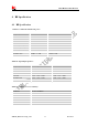
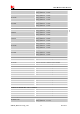
Table 21: Electronic Characteristics
Specification
Min Typ Max Unit Comments/Conditions
Resolution 12 Bits
Differential nonlinearity -4 +4 LSB
Integral nonlinearity -8 +8 LSB
Gain Error -2.5 +2.5 %
Offset Error -4 +40 LSB
Analog Vdd = ADC reference
2.4MHz sample rate
Input Range GND 2.2V V
Input serial resistance 2 kΩ Sample and hold switch resistance
Input capacitance 53 pF
Power-down to wakeup 9.6 19.2 μs
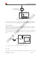
User can introduce a signal in the ADC pin directly and use the AT command “AT+CADC” to get the raw
data which is between 0 and 255. The data can be transformed to any type such as voltage, temperature etc.
Please refer to Chapter 3.1.2 and document [1].
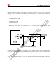
Figure 31: Reference circuit
Note: The input signal voltage value in ADC must not be higher than 2.2V.
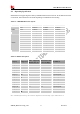
3.10.4 LDO
SIM5320AD has a LDO power output, namely VREG_AUX. The LDO is available and output voltage is
2.85v by default, rated for 250mA. User can switch the LDO on or off by the AT command
“AT+CVAUXS” and configure its output voltage by the AT command “AT+CVAUXV”.
Table 22: Electronic characteristic
Symbol Description Min Typ Max Unit
VREG_AUX Output voltage 1.5 2.85 3.05 V
I
O
Output current - - 250 mA