
User's Manual

Smart Machine Smart Decision
SIM5320_Hardware Design_V1.01 2011-11-10
7
Figure Index
Figure 1: SIM5320AD functional architecture................................................................................................................ 10
Figure 2: Pin view........................................................................................................................................................... 12
Figure 3: Top dimensions (Unit: mm)............................................................................................................................. 16
Figure 4: Side dimensions (Unit: mm)............................................................................................................................ 17
Figure 5: Bottom dimensions (Unit: mm) ....................................................................................................................... 17
Figure 6: Footprint recommendation (Unit: mm)............................................................................................................ 18
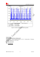
Figure 7: VBAT_RF voltage drop during burst emission (GSM/GPRS)......................................................................... 19
Figure 8: VBAT input application circuit........................................................................................................................ 20
Figure 9: Reference circuit of the LDO power supply .................................................................................................... 20
Figure 10: Reference circuit of the DCDC power supply ............................................................................................... 21
Figure 11: RTC supply from capacitor............................................................................................................................ 22
Figure 12: RTC supply from non-chargeable battery...................................................................................................... 22
Figure 13: RTC supply from rechargeable battery .......................................................................................................... 22
Figure 14: Seiko XH414H-IV01E Charge-Discharge characteristic............................................................................... 23
Figure 15: Power on Timing Sequence ........................................................................................................................... 24
Figure 16: Application circuit ......................................................................................................................................... 25
Figure 17: Power off timing sequence ............................................................................................................................ 26
Figure 18: Full modem.................................................................................................................................................... 27
Figure 19: Null modem ................................................................................................................................................... 27
Figure 20: RI behaviour in NULL Modem ..................................................................................................................... 28
Figure 21: RI behaviour in FULL Modem ...................................................................................................................... 29
Figure 22: USIM interface reference circuit ................................................................................................................... 30
Figure 23: Amphenol SIM card socket ........................................................................................................................... 31
Figure 24: USB interface ................................................................................................................................................ 33
Figure 25: Application circuit ......................................................................................................................................... 35
Figure 26: Flight mode switch ........................................................................................................................................ 36
Figure 27: Active antenna circuit .................................................................................................................................... 38
Figure 28:Passive antenna circuit (Default) ................................................................................................................. 38
Figure 29: Current drive.................................................................................................................................................. 40
Figure 30: Reset circuit................................................................................................................................................... 40
Figure 31: Reference circuit............................................................................................................................................ 41
Figure 32: Antenna matching circuit............................................................................................................................... 44
Figure 33: Top and bottom view of SIM5320AD ........................................................................................................... 50
Figure 34: The ramp-soak-spike reflow profile of SIM5320AD..................................................................................... 50
Figure 35: Recommended pad ........................................................................................................................................ 51
Figure 36: System design................................................................................................................................................ 52