
User's Manual
Smart Machine Smart Decision
SIM5320A_Hardware Design_V1.01 2011-2-29
54
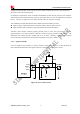
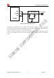
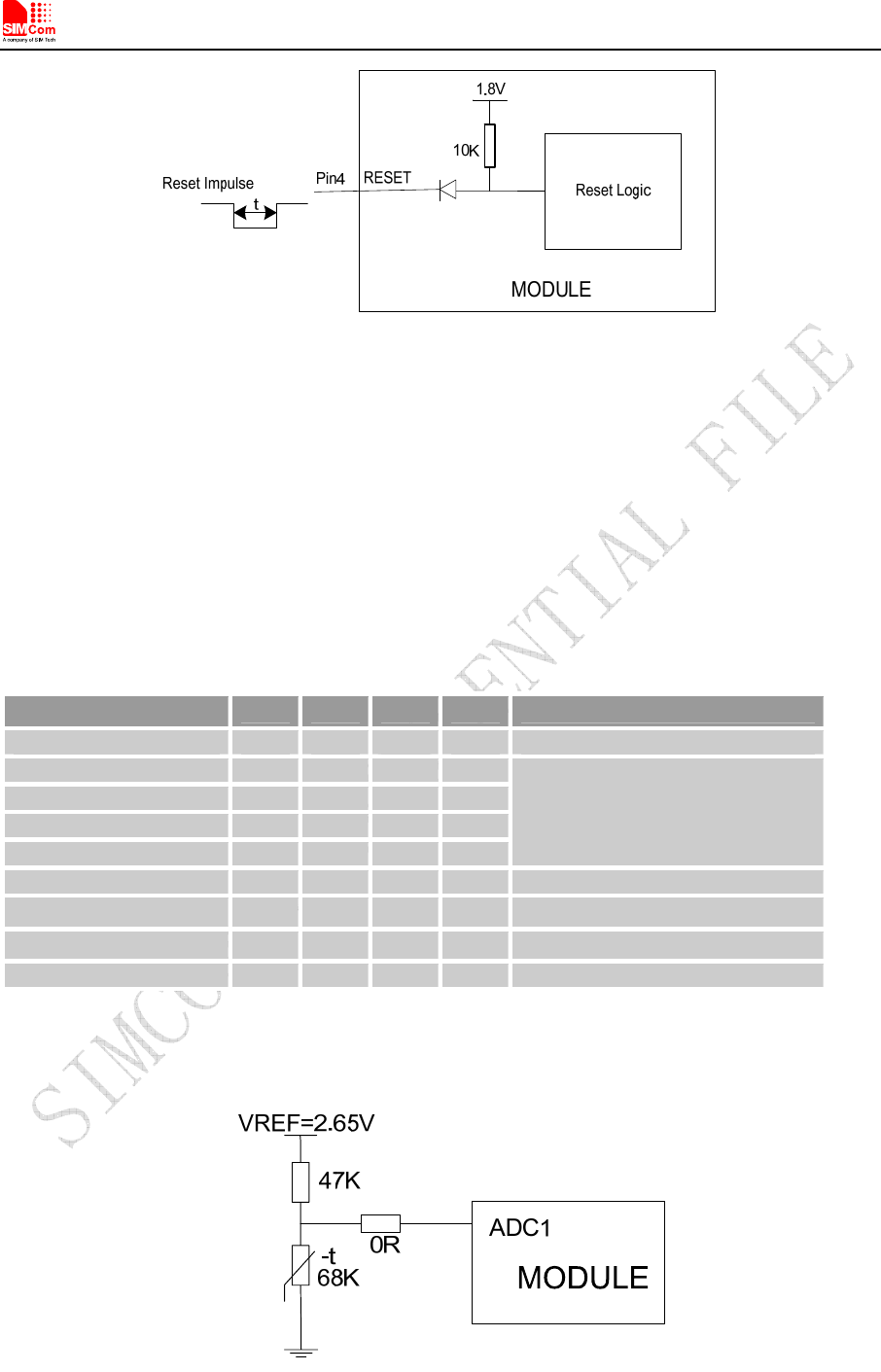
Figure 42: Reset circuit
Note
:
50ms<t<200ms. ESD components are suggested to be used on Reset pin.
3.13.3 ADC
SIM5320A has a dedicated ADC that is available for digitizing analog signals such as battery voltage and
so on; it is on PIN 47, namely ADC1. This ADC1 is 8 bit successive-approximation circuit, and electronic
specification is shown in the following table.
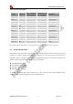
Table 33: Electronic Characteristics
Specification
Min Typ Max Unit Comments/Conditions
Resolution 8 Bits
Differential nonlinearity -4 +4 LSB
Integral nonlinearity -8 +8 LSB
Gain Error -2.5 +2.5 %
Offset Error -4 +40 LSB
Analog Vdd = ADC reference
2.4MHz sample rate
Input Range GND 2.2V V
Input serial resistance 2 kΩ Sample and hold switch resistance
Input capacitance 53 pF
Power-down to wakeup 9.6 19.2 μs
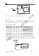
User can introduce a signal in the ADC pin directly and use the AT command “AT+CADC” to get the raw
data which is between 0 and 255. The data can be transformed to any type such as voltage, temperature etc.
Please refer to Chapter 3.1.2 and document [1].
Figure 43: Reference circuit