
User's Manual
Smart Machine Smart Decision
SIM5320A_Hardware Design_V1.01 2011-2-29
22
3.1.2 Design Guide
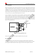
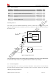
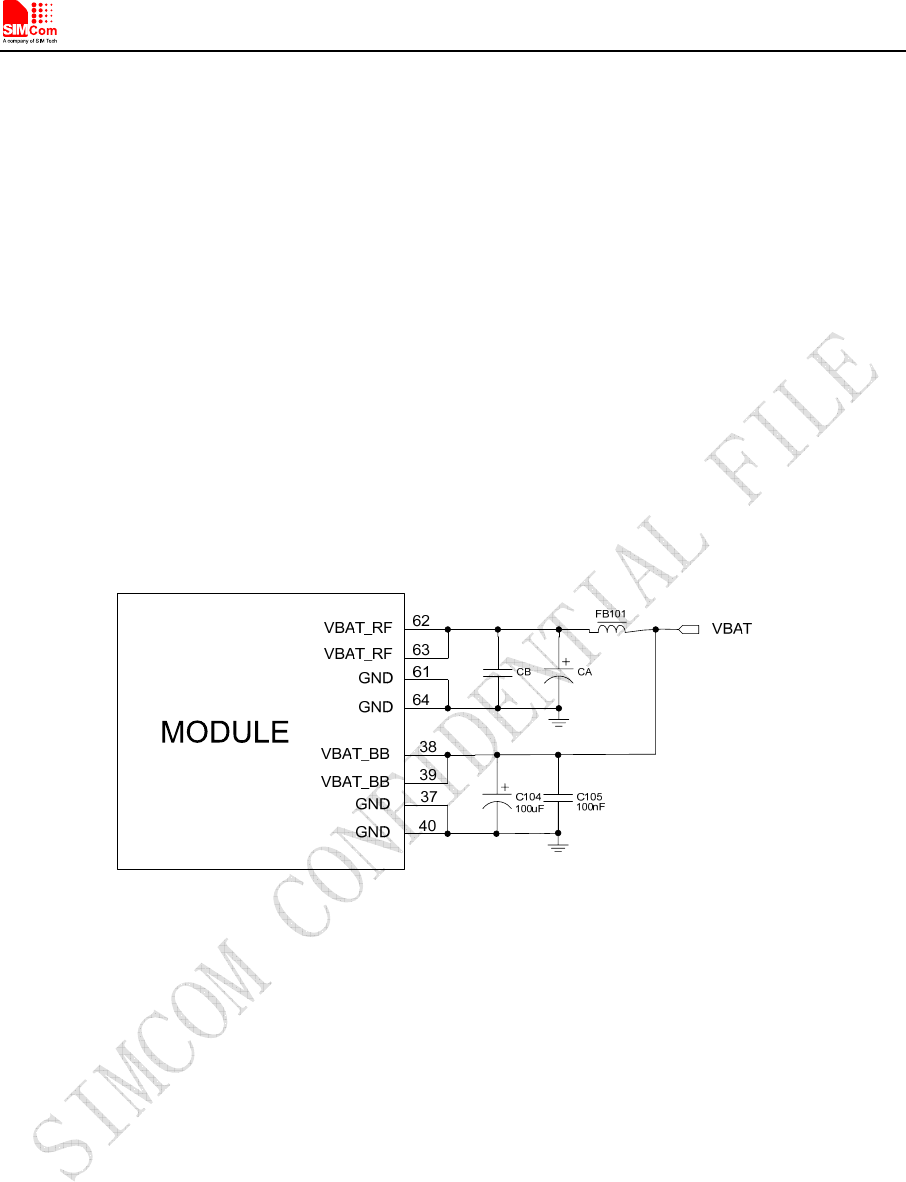
Mostly, user connects the VBAT_RF and VBAT_BB pins with one power supply. Make sure that the input
voltage at the VBAT_BB pin will never drop below 3.3V even during a transmit burst when the current
consumption rises up to 2A. If the power voltage drops below 3.3V, the module may be shut down
automatically. Using a large tantalum capacitor (above 100uF) will be the best way to reduce the voltage
drops. If the power current cannot support up to 2A, users must introduce larger capacitor (typical 1000uF)
to storage electric power, especially GPRS multiple time slots emission.
For the consideration of RF performance and system stability, another large capacitor (above 100uF)
should be located at the VBAT_RF pin and some multi-layer ceramic chip (MLCC) capacitors (0.1uF)
need to be used for EMC because of their low ESR in high frequencies. Note that capacitors should be put
beside VBAT_RF pins as close as possible. Also User should minimize the PCB trace impedance from the
power supply to the VBAT pins through widening the trace to 80 mil or more on the board. The following
figure is the recommended circuit.
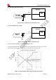
Figure 8: VBAT input application circuit
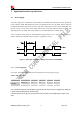
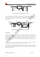
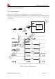
There are three sections about how to design and optimize users’ power systems.
Power supply circuit
We recommend DCDC or LDO is used for the power supply of the module, make sure that the peak
current of power components can rise up to 2A. The following figure is the reference design of +5V input
power supply. The designed output for the power supply is 4.1V, here a linear regulator can be used.