
Installation Instructions

SIM5216A _HD_V1.02 Hardware Design
SIM5216A _HD_V1.02 26.08.2010
44
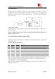
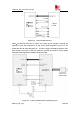
■ 8 bit data bus for the pixel data information
■ Horizontal and vertical synchronization signals
■ 2 wire I2C bus as a control path between the SIM5216A module device and the camera module
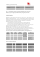
The following table is the pin definition.
Table 24: PIN define of sensor interface
We have tested several kinds of digital sensors, such as OV2640, OV7670,OV7725 and a
NTSC/PAL digital video decoder named AK8856 (it can decode NTSC or PAL composite video
signals into digital video data, and with AK8856 you can use analog sensor as video source) .
Software must be adjusted when use other kinds of sensors. Customer can contact us and give us
your request. The power supply of the sensor should be supplied by customer.
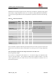
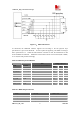
Pin Name Function
15 CAM_D2 Bit 0 of RGB or YUV D0 video component output
54 CAM_D3 Bit 1 of RGB or YUV D1 video component output
16 CAM_D4 Bit 2 of RGB or YUV D2 video component output
53 CAM_D5 Bit 3 of RGB or YUV D3 video component output
17 CAM_D6 Bit 4 of RGB or YUV D4 video component output
52 CAM_D7 Bit 5 of RGB or YUV D5 video component output
18 CAM_D8 Bit 6 of RGB or YUV D6 video component output
51 CAM_D9 Bit 7 of RGB or YUV D7 video component output
19 CAM_HSYNC Video horizontal line synchronization signal
50 CAM_VSYNC Vertical sync output
21 CAM_CLK master clock input
49 CAM_PCLK Pixel clock output
48 CAM_RESET Master reset input, active low
47 IIC_SDA Serial interface data input and output
46 IIC_SCL Serial interface clock input
20 GND Ground
22 CAM_STANDBY Power-down mode selection
“0”=Normal mode, “1”=Power-down mode