
User's Manual

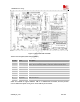
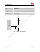

Table Of Contents
- Contents
- Version history
- 1 Introduction
- 2 SIM900B Overview
- 3 Application Interface
- 3.1 SIM900B Pin Description
- 3.2 Operating Modes
- 3.3 Power Supply
- 3.4 Power Up and Power Down Scenarios
- 3.5 Power Saving
- 3.6 Summary of State Transitions (except SLEEP mode)
- 3.7 RTC Backup
- 3.8 Serial Interfaces
- 3.9 Audio Interfaces
- 3.10 Buzzer
- 3.11 SIM Card Interface
- 3.12 LCD Display Interface
- 3.13 Keypad Interface
- 3.14 ADC
- 3.15 Behaviors of the RI
- 3.16 Network Status Indication
- 3.17 General Purpose Input Output (GPIO)
- 4 Antenna Interface
- 5 Electrical, Reliability and Radio Characteristics
- 6 Mechanics

SIM900B Hardware Design
4 Antenna Interface
The RF interface has an impedance of 50Ω. To suit the physical design of individual applications, SIM900B
offers alternatives:
z Recommended approach: antenna connector on the component side of the PCB
z Antenna pad and grounding plane placed on the bottom side.
Figure 32 : The RF interface of module
The antenna can be soldered to the pad, or attached via contact springs. To help you to ground the antenna,
SIM900B comes with a grounding plane located close to the antenna pad.
SIM900B material properties:
SIM900B PCB Material: FR4
Antenna pad: Gold plated pad
To minimize the loss on the RF cable, it need be very careful to choose RF cable. We recommend the insertion
loss should be meet following requirements:
z GSM900<1dB
z DCS1800/PCS1900<1.5dB
SIM900B_HD_V1.03 24.06.2010
49