
User's Manual

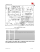
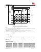
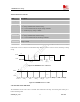
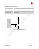
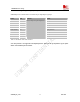

Table Of Contents
- Contents
- Version history
- 1 Introduction
- 2 SIM900B Overview
- 3 Application Interface
- 3.1 SIM900B Pin Description
- 3.2 Operating Modes
- 3.3 Power Supply
- 3.4 Power Up and Power Down Scenarios
- 3.5 Power Saving
- 3.6 Summary of State Transitions (except SLEEP mode)
- 3.7 RTC Backup
- 3.8 Serial Interfaces
- 3.9 Audio Interfaces
- 3.10 Buzzer
- 3.11 SIM Card Interface
- 3.12 LCD Display Interface
- 3.13 Keypad Interface
- 3.14 ADC
- 3.15 Behaviors of the RI
- 3.16 Network Status Indication
- 3.17 General Purpose Input Output (GPIO)
- 4 Antenna Interface
- 5 Electrical, Reliability and Radio Characteristics
- 6 Mechanics

SIM900B Hardware Design
KBR4
KBR3
KBR2
KBR1
KBC0
KBC1
KBC2
KBC3
KBC4
GND
MODULE
Figure 28: Reference circuit of the keypad interface
*Note:
1. This function is not supported in the default firmware. There must be customized firmware if you want.
Please contact SIMCom for more details.
2.KBR0&KBC0 is used to power off the module, so do not connect them for other application.
3. keypad is the second function of this pin , the default function is GPIO.
3.14 ADC
SIM900B provides one auxiliary ADC (General purpose analog to digital converter.) as voltage input pin, which
can be used to detect the values of some external items such as voltage, temperature etc. We can use AT
command “AT+CADC” to read the voltage value on ADC. For detail of this AT command, please refer to
document [1].
Table 18: ADC specification
MIN Type MAX Units
Voltage range 0 - 2.8 V
ADC Resolution - 10 - bits
Sampling rate - - 200K Hz
SIM900B_HD_V1.03 24.06.2010
45