
User's Manual

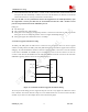


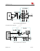

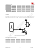
Table Of Contents
- Contents
- Version history
- 1 Introduction
- 2 SIM900B Overview
- 3 Application Interface
- 3.1 SIM900B Pin Description
- 3.2 Operating Modes
- 3.3 Power Supply
- 3.4 Power Up and Power Down Scenarios
- 3.5 Power Saving
- 3.6 Summary of State Transitions (except SLEEP mode)
- 3.7 RTC Backup
- 3.8 Serial Interfaces
- 3.9 Audio Interfaces
- 3.10 Buzzer
- 3.11 SIM Card Interface
- 3.12 LCD Display Interface
- 3.13 Keypad Interface
- 3.14 ADC
- 3.15 Behaviors of the RI
- 3.16 Network Status Indication
- 3.17 General Purpose Input Output (GPIO)
- 4 Antenna Interface
- 5 Electrical, Reliability and Radio Characteristics
- 6 Mechanics

SIM900B Hardware Design
Name Pin Function
DCD 28 Data carrier detection
DTR 38 Data terminal ready
RXD 40 Receive data
TXD 42 Transmit data
RTS 44 Request to send
CTS 46 Clear to send
Serial port
RI 48 Ring indicator
DBG_RXD 47 Receive data
Debug port
DBG_TXD 49 Transmit data
SIM900B provides two unbalanced asynchronous serial ports. One is the serial port and the other is the debug port.
The GSM module is designed as a DCE (Data Communication Equipment), following the traditional DCE-DTE
(Data Terminal Equipment) connection. The module and the client (DTE) are connected through the following
signal (as following figure shows). Autobauding supports baud rate from 1200bps to 57600bps.
Serial port
z TXD: Send data to the RXD signal line of the DTE
z RXD: Receive data from the TXD signal line of the DTE
Debug port
z DBG_TXD: Send data to the RXD signal line of the DTE
z DBG_RXD: Receive data from the TXD signal line of the DTE
The logic levels are described in following table.
Table
8: Logic levels of the serial port and debug port
Parameter Min Max Unit
V
IL
0 0.15*VDD_EXT V
V
IH
0.85 *VDD_EXT VDD_EXT V
V
OL
0 0.1 V
V
OH
VDD_EXT -0.1 VDD_EXT V
SIM900B_HD_V1.03 24.06.2010
32