
User's Manual
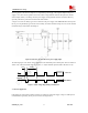
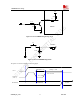
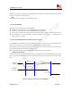


Table Of Contents
- Contents
- Version history
- 1 Introduction
- 2 SIM900B Overview
- 3 Application Interface
- 3.1 SIM900B Pin Description
- 3.2 Operating Modes
- 3.3 Power Supply
- 3.4 Power Up and Power Down Scenarios
- 3.5 Power Saving
- 3.6 Summary of State Transitions (except SLEEP mode)
- 3.7 RTC Backup
- 3.8 Serial Interfaces
- 3.9 Audio Interfaces
- 3.10 Buzzer
- 3.11 SIM Card Interface
- 3.12 LCD Display Interface
- 3.13 Keypad Interface
- 3.14 ADC
- 3.15 Behaviors of the RI
- 3.16 Network Status Indication
- 3.17 General Purpose Input Output (GPIO)
- 4 Antenna Interface
- 5 Electrical, Reliability and Radio Characteristics
- 6 Mechanics

SIM900B Hardware Design
The circuit design of the power supply depends strongly upon the power source where this power is drained. The
following figure is the reference design of +5V input source power supply. The designed output for the power
supply is 4.1V, thus a linear regulator can be used. If there’s a big difference between the input source and the
desired output (VBAT), a switching converter power supply will be preferable because of its better efficiency
especially with the 2A peak current in burst mode of the module.
A single 3.6V Li-Ion cell battery type can be connected to the power supply of the SIM900B VBAT directly. But
the Ni_Cd or Ni_MH battery types must be used carefully, since their maximum voltage can rise over the absolute
maximum voltage of the module and damage it.
Figure 4: Reference circuit of the source power supply input
The following figure is the VBAT voltage ripple wave at the maximum power transmit phase, the test condition is
VBAT=4.0V, VBAT maximum output current =2A, C
A
=100µF tantalum capacitor (ESR=0.7Ω) and C
B
=1µF.
Max:300mV
VBAT
Burst:2A
IVBAT
4.615ms
577us
Figure 5: VBAT voltage drop during transmit burst
3.3.1 Power Supply Pins
Eight VBAT pins of the board-to-board connector are dedicated to connect the supply voltage; six GND pins are
recommended for grounding. VRTC pin can be used to back up the RTC.
SIM900B_HD_V1.03 24.06.2010
23