
User Guide

SMT Module RF Reference Design Guide
SMT Module RF Reference Design Guide 7
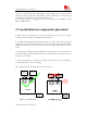
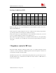
Stack-up of eight-layers PCB
Top
layer
Second
layer
Third
layer
Forth
layer
Fifth
layer
Sixth
layer
Seventh
layer
Bottom
layer
A S1 S2 GND S3 S4 POWER
S5 S6
B S1 S2 S3 GND POWER
S4 S5 S6
C S1 GND S2 S3 S4 S5 POWER
S6
D S1 GND S2 S3 GND POWER
S4 S5
E S1 GND S2 GND S3 POWER
S4 S5
F S1 GND S2 GND POWER
S3 GND S4
Table4 Stack-up of eight-layers PCB
Eight-layers PCB gives more design flexibility than a six-layers PCB, but it takes some work to
make it ideal in EMC terms.
If the design needs 6 signal routing layers, then case A will be the best stack-up design, but this
type stack-up should not be used in high speed digital circuit design.
If the product design needs 5 signal routing layers, case E will be the best. In this case, S1, S2 and
S3 are good signal routing layer, and the power decoupling is good.
If the design needs 4 signal routing layers, case F will be the best. In this case, every signal routing
layers are good. In all the case, the signal trace routed in adjacent signal routing layers should be
orthogonal.
5 Impedance control of RF trace
Because the module’s RF part is working in a 50ohm system, so its output load impedance should
be 50ohm, to meet this requirement, the all RF signal trace should be impedance controlled, and
its characteristic impedance should be 50ohm.
The RF trace impedance can be controlled through using different trace geometry. There are more
than thirty different types of transmission line which can easily be created on a PCB. Twelve of
them are shown in figure 7