
User Guide

SMT Module RF Reference Design Guide
SMT Module RF Reference Design Guide 5
VBAT
VBAT
VBAT
55
57
56
RF_IN
60
GND
GND61
59
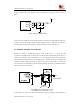
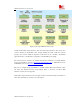
Figure3 is the best placement; antenna part is near RF_IN pad, power supply is near VBAT pad,
noise source is far away the Sim900.
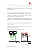
Figure4, Figure5, Figure6 are bad placements. Figure4, power supply and antenna part are crossed;
Figure5, noise source is near to Sim900; Figure6 antenna part is far away from RF_IN pad of
sim900.
4 Stacking up of multi-layers PCB
For EMC performance consideration, once the working frequency in the customer’s product is
over than 5MHz, or the rise-up/fall-down period of digital signal is less than 5ns, then multi-layers
PCB should be considered. Now, the more common multi-layer PCB structure is four-layers,
six-layers and eight-layers PCB, etc. If the customer’s product is designed in multi-layers PCB
technology, then the stack-up design of multi-layers PCB will become very important. The
following will show some typical stack-up design of multi-layers PCB, but each design has its
own advantages and disadvantages.
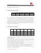
Note: In the following table, S1 indicates the first signal layer, S2 indicates the second signal
layer, and so on.
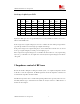
Stack-up of two-layers PCB
Top layer Bottom layer
Case A S1+POWER+GND S2+POWER+GND
Table1 Stack-up of two-layers PCB