
User Guide

SMT Module RF Reference Design Guide
SMT Module RF Reference Design Guide 4
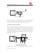
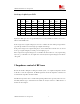
add the optional component R3, then a T-type matching circuit structure will be made up with
another two components R4 and C5. But usually, a pi-type matching circuit is enough in antenna
tuning process. The component J2 is a RF test Port, used for conduct RF test. The traces in Bold
type must be 50 ohm impedance controlled when layout a design.
For the RF test connector, we suggested the customer use the part vended by Murata, its part
number is MM8430-2610.
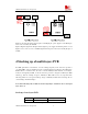
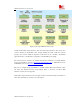
3 Consideration in components placement
In PCB design, a good placement of components will help the improving of the product’s
performance. The following are some thumbs should be followed.
1)The SMT module should be placed far away from the noise source circuit, such as high speed
digital circuit, etc. if this requirement cannot be met, the noise source circuit should be shielded
perfectly. This will help to reduce the interference between the SMT module and the noise source
circuit.
2)The placement of SMT module should make the module’s RF port close to the antenna’s feed
pad. This will make the length of RF trace between the module’s RF port and antenna as short as
possible, and consequently.
3)The decoupling capacitor of module’s power supply should be placed close to the VBAT pads,
this will help the improvement of decoupling.
The best placement and some bad placements are shown as below:
SIM900
Figure3 Good Placement
Antenna
Matching circuit
and Antenna area
Power Supply
Noise Source
(high speed
digital circuit, or
others)