
User Guide
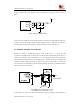

SMT Module RF Reference Design Guide
SMT Module RF Reference Design Guide 1
SMT Module RF Reference Design Guide
1 Introduction....................................................................................................................................2
2 Circuit design .................................................................................................................................2
2.1 Power supply circuit design ................................................................................................2
2.2 Antenna matching circuit design.........................................................................................3
3 Consideration in components placement........................................................................................4
4 Stacking up of multi-layers PCB....................................................................................................5
Stack-up of two-layers PCB......................................................................................................5
Stack-up of four-layers PCB .....................................................................................................6
Stack-up of six-layers PCB .......................................................................................................6
Stack-up of eight-layers PCB....................................................................................................7
5 Impedance control of RF trace.......................................................................................................7
6 Consideration in PCB layout........................................................................................................10
Appendix......................................................................................................................................... 11
Two-layers PCB ...................................................................................................................... 11
Four-layers PCB......................................................................................................................12
Six-layers PCB........................................................................................................................13
Eight-layers PCB.....................................................................................................................16
Version History
Data Version
Description of change Author
2010-1-20 01.01 Origin Ye Haibing,
Wang Guoqiang