
User Guide
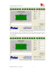

SMT Module RF Reference Design Guide
SMT Module RF Reference Design Guide 11
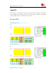
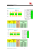
Appendix
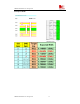
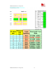
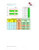
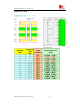
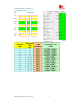
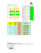
The following are some illustration of impedance controlled RF trace designing. It is should be
noted that the RF trace’s width and spacing to the reference ground is combined to specific PCB
stack-up(the PCB’s thickness, clearance between every layer).
Two-layers PCB