
User Guide

SMT Module RF Reference Design Guide
SMT Module RF Reference Design Guide 10
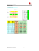
6 Consideration in PCB layout
In product’s PCB design, a good PCB layout will help the improvement of the whole product
performance, including reliability, EMC performance, etc. The following are some considerations
for referenced:
a) The Layer1.under SMT module test port should be copper keep out , layer2 should be GND;
b) The Layer2 under SMT module RF_IN pad should be copper keep out , layer3 should be
GND;
c) The Layer1.Layer2 under RF test connector should be copper keep out, layer3 should be GND;
the space to GND plane should more than 0.5mm.
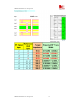
d) RF trace between SMT module RF pad with the RF test connector, RF trace between RF test
connector with the antenna matching circuit, RF trace between the antenna matching circuit
with the antenna feed PAD all should be controlled to 50 Ohm
e) Avoid to layout any high speed signal under RF trace, if high speed signal is needed, a GND
plane is needed between these two signals.
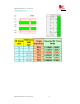
f) All layers under the antenna feed pad should be copper keep out. Or, the space between
antenna feed pad with the GND under feed pad should be more than 1mm.
g) Do not layout RF trace in orthogonal.
h) When layout surface Mircostrip Transmission Line or offset Strip Transmission Line , 3W
rule should be followed, that means the space between reference GND with RF trace should
three times more than the width of RF trace.