SMT Module RF Reference Design Guide AN_ SMT Module RF Reference Design Guide _V1.
Document Title: SMT Module RF Reference Design Guide Version: 1.01 Date: 2010-1-27 Status: Release Document Control ID: AN_SMT Module RF Reference Design Guide_V1.01 General Notes SIMCOM offers this information as a service to its users, to support application and engineering efforts that use the products designed by SIMCOM. The information provided is based upon requirements specifically provided to SIMCOM by the users.
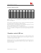
SMT Module RF Reference Design Guide SMT Module RF Reference Design Guide 1 Introduction....................................................................................................................................2 2 Circuit design .................................................................................................................................2 2.1 Power supply circuit design ................................................................................................2 2.
SMT Module RF Reference Design Guide 1 Introduction This document describes the important points about RF that should be taken into account in client’s application design. As SMT module can be integrated with a wide range of applications, the application notes are described in detail. SMT module is a new and key product which is provided by SIMCom inc. This type module become very popular soon after it is released for its easy integration, good reliability.
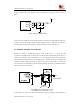
SMT Module RF Reference Design Guide spectrum, switching spectrum, a series large current ferrite bead(with rated current minimum 2A) should be added at the power supply port. The recommended power supply circuit is shown as below: VBAT VBAT 55 VBAT 56 VBAT 57 R1 C3 C2 C1 22pF 100nF 100uF SIM900 Figure1 Power Supply Circuit In this circuit, by default, the component R1 should be a 0ohm resistor with 0805 size.
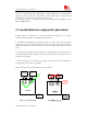
SMT Module RF Reference Design Guide add the optional component R3, then a T-type matching circuit structure will be made up with another two components R4 and C5. But usually, a pi-type matching circuit is enough in antenna tuning process. The component J2 is a RF test Port, used for conduct RF test. The traces in Bold type must be 50 ohm impedance controlled when layout a design. For the RF test connector, we suggested the customer use the part vended by Murata, its part number is MM8430-2610.
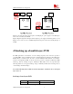
SMT Module RF Reference Design Guide 55 VBAT 56 VBAT 57 VBAT 59 GND 60 RF_IN 61 GND Figure3 is the best placement; antenna part is near RF_IN pad, power supply is near VBAT pad, noise source is far away the Sim900. Figure4, Figure5, Figure6 are bad placements. Figure4, power supply and antenna part are crossed; Figure5, noise source is near to Sim900; Figure6 antenna part is far away from RF_IN pad of sim900.
SMT Module RF Reference Design Guide Two-layers PCB is the lowest cost solution, but this solution has the worst EMC performance, and it is not appropriate in high speed design, because in this solution, the ground integrity, the crosstalk between signal traces is very bad.
SMT Module RF Reference Design Guide Stack-up of eight-layers PCB Top layer Second layer Third layer Forth layer Fifth layer Sixth layer Seventh layer Bottom layer A S1 S2 GND S3 S4 POWER S5 S6 B S1 S2 S3 GND POWER S4 S5 S6 C S1 GND S2 S3 S4 S5 POWER S6 D S1 GND S2 S3 GND POWER S4 S5 E S1 GND S2 GND S3 POWER S4 S5 F S1 GND S2 GND POWER S3 GND S4 Table4 Stack-up of eight-layers PCB Eight-layers PCB gives more design flexibility than a six-layers
SMT Module RF Reference Design Guide Figure7 twelve typical PCB transmission line Usually, Surface Mircostrip Transmission Line and offset Strip Transmission Line are the most common structures. In 50ohm RF system, through adjusting the width of RF traces and the spacing to the reference GND, the impedance of RF traces can be controlled to 50Ohm.The appendix will show some illustration in impedance controlled RF trace designing.
SMT Module RF Reference Design Guide Figure8 Surface Mircostrip Calculate Offset Strip Transmission Line,the height between two reference GND is 418um (203+35+180 = 418um), the height between RF trace and reference GND is 180um, the result width is 135um. as shown in figure9.
SMT Module RF Reference Design Guide 6 Consideration in PCB layout In product’s PCB design, a good PCB layout will help the improvement of the whole product performance, including reliability, EMC performance, etc. The following are some considerations for referenced: a) The Layer1.under SMT module test port should be copper keep out , layer2 should be GND; b) The Layer2 under SMT module RF_IN pad should be copper keep out , layer3 should be GND; c) The Layer1.
SMT Module RF Reference Design Guide Appendix The following are some illustration of impedance controlled RF trace designing. It is should be noted that the RF trace’s width and spacing to the reference ground is combined to specific PCB stack-up(the PCB’s thickness, clearance between every layer).
SMT Module RF Reference Design Guide Four-layers PCB SMT Module RF Reference Design Guide 12
SMT Module RF Reference Design Guide Six-layers PCB SMT Module RF Reference Design Guide 13
SMT Module RF Reference Design Guide SMT Module RF Reference Design Guide 14
SMT Module RF Reference Design Guide SMT Module RF Reference Design Guide 15
SMT Module RF Reference Design Guide Eight-layers PCB SMT Module RF Reference Design Guide 16
SMT Module RF Reference Design Guide SMT Module RF Reference Design Guide 17
SMT Module RF Reference Design Guide Contact us: Shanghai SIMCOM Wireless Solutions Ltd Add: SIM Technology Building, No. 633, JinZhong Road, Shanghai,PRChina 200335 Tel: +86 21 32523300 Fax: +86 21 32523200 URL:www.sim.