
User's Manual


1.2. Electrical Parameters
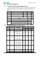
1.2.1. Absolute maximum ratings: Voltage & Current
Stresses above the absolute maximum ratings may cause permanent damage to the device.
These are stress ratings only and functional operation of the device at these conditions is not
implied. Exposure to maximum rating conditions for extended periods may affect device
reliability.
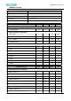
Symbol
Ratings
Min
Max
Unit
V
DD
–V
SS
Voltage
–0.3
4.0
V
V
IN
Input voltage on five volt tolerant pin
VSS −0.3
5.5
V
V
IN
Input voltage on any other pin
VSS −0.3
VDD+0.3
V
Symbol
Ratings
Max
Unit
I
VDD
Total current into VDD power lines (source)
320
mA
I
VSS
Total current out of VSS ground lines (sink)
320
mA
I
IO
Output current sunk by any I/O and control pin
25
mA
I
IO
Output current source by any I/Os and control pin
-25
mA
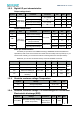
1.2.2. Operating conditions: Voltage & Current
Symbol
Note
Conditions
Specification
Specification
Specification
Specification
Symbol
Note
Conditions
Min.
Typical
Max.
Unit
DD
I
VDD
Current
VDD=3.3V, normal
2437 MHz,18 dBm,
11 Mbps CCK
TX Speed:80kbytes/s
219
224
230
mA
I
VDD
Current
VDD=3.3V, normal
2437 MHz,18 dBm,
11 Mbps CCK
TX Speed:10kbytes/s
199
202
204
mA
I
VDD
Current
VDD=3.3V, normal
2437 MHz,15 dBm,
54 Mbps OFDM
TX Speed:80kbytes/s
203
204
205
mA
I
VDD
Current
VDD=3.3V, normal
2437 MHz,15 dBm,
54 Mbps OFDM
TX Speed:10kbytes/s
199
200
202
mA
I
VDD
Current
VDD=3.3V,Receive mode
182
185
188
mA
I
VDD
Current
VDD=3.3V,Sleep mode
50
60
uA
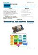
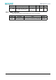
! ! EMW3280 Wi-Fi module
2
V Voltage 3.0 3.3 3.5 V