Track Number: AN0049EN MXCHIP Co., Ltd Version: 0.5 2016.12.8 Category: Application Note Open User Manual of EMW3239 Abstract This document lists the consideration in each step during designing product with MXCHIP module. In order to achieve rapid mass production, Users should be familiar with the document to pre-consider and avoid problems effectively in designing, producing, programming and testing. More Help For more products information please visit: http://mxchip.
Application Note [Page 1] Version Record Date Version 2016-9-23 0.1 Details Initial document Add reference circuit 2016-9-29 0.2 Add description of pin function and design consideration Add position figure of PCB 2016-12-2 0.3 Add Module downloading method 2016-12-6 0.4 Add module testing method 2016-12-8 0.
Application Note [Page 2] Content User Manual of EMW3239 ................................................................................................................................................ 1 Version Record .................................................................................................................................................................... 1 1. Introduction............................................................................................................
Application Note [Page 3] Figure 2.3 SMT Package ..................................................................................................................................... 7 Figure 2.4 PCB Design ........................................................................................................................................ 9 Figure 2.5 Minimum PCB Clearance Area ........................................................................................................ 10 Figure 2.
Application Note [Page 4] 1. Introduction This document lists the consideration in each step during designing product with MXCHIP module. In order to achieve rapid mass production, Users should be familiar with the document to pre-consider and avoid problems effectively in designing, producing, programming and testing. Suitable module type: EMW3239 Phase of attention: Hardware design; Firmware testing; SMT; Online update.
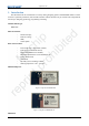
Application Note Module type Antenna type Illustration EMW3239-P On-board PCB Antenna Default EMW3239-E IPEX brass pipe Antenna Optional [Page 5] Manufacture Dongguan Aosiya Antenna Technology Co.,Ltd Dongguan Aosiya Antenna Technology Co.
Datasheet [Page 7] 1.1 Pin arrangement EMW3239 has 41 pins in two rows (1x20 and 1x21) with 0.8mm pitch. Stamp hole package interface design is used in EMW3239 (as shown in figure 3) to simplify debugging and disassembling for developers, as well as offering varied selection. Also it is benefit for SMT patch and hand-welding. Solder mask openness has the same size with land. The width of steel mesh is suggested to be 0.12mm to 0.14mm in SMT.
Datasheet [Page 9] 1.2 Pin Definition 1.2.
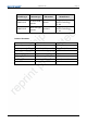
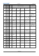
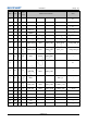
Datasheet Pins Name Type I/O Level [Page 10] Multi-select Function User I2S2_CK √ 6 PB13 I/O FT SPI2_SCK GPIO CAN2_TX 7 PB14 I/O FT SPI2_MISO GPIO TIM12_CH1 8 PC6 I/O FT UART6_TXD GPIO TIM3_CH1 I2S2_MCK 9 PA15 I/O FT GPIO JTDI TIM2_CH1 USART1_TXD 10 VBAT S - VBAT 11 - - - 12 PC7 I/O FT UART6_RXD 13 NRST I/O FT RESET 14 PC0 I TC GPIO 15 - - - 16 PC13 I/O FT GPIO 17 PB8 I/O FT I2C1_SCL GPIO TIM4_CH3 CAN1_RX √ 18 PB9 I/O FT I2
Datasheet Pins Name Type I/O Level [Page 11] Multi-select Function User 22 - - - NC 23 - - - NC 24 - - - NC 25 PA14 I/O FT SWCLK × 26 PA13 I/O FT SWDIO × 27 PB3 I/O FT GPIO 28 - - - 29 PB7 I/O FT UART1_RXD GPIO TIM4_CH2 I2C1_SDA √ USER_UART_RX 30 PB6 I/O FT UART1_TXD GPIO TIM4_CH1 I2C1_SCL √ USER_UART_TX 31 PB4 I/O FT GPIO JTRST TIM3_CH1 32 - - - 33 PA10 I/O FT USB_ID 34 PA5 I/O TC GPIO 35 PA11 I/O FT USB_DM GPIO 36 PA1
Datasheet [Page 12] Illustration: 1. Pin 10, pin 39 and pin 40 should be connected to VDD 3V3, pin 20 and pin 21 should be connected to ground; 2. Pin 8 and pin 12 could only be used in secondary write, ATE or QC automatic detection; 3. Pin 29 and pin 30 is used as serial communication in bootloader mode for users; 4. S stands for power supply, I stands for input pins and I/O stands for input and output pins; 5.
Application Note 2. Considerations in Hardware Design 2.1 Mechanical Size Mechanical size of EMW3031(Unit: mm) Figure 2.1 Top View of Mechanical Size Figure 2.2 Side View of Mechanical Size 2.2 Reference Package Design Solder mask openness has the same size with land, as shown in figure2.
Application Note [Page 7] Figure 2.3 SMT Package 2.3 DC Power Design Peak current of the module is approximately 360mA. DC/DC with maximum output current 600mA is suggested as power supply. DC/DC is better than LDO in low power consumption. Route should be particularly aware for DC/DC power supply. Compact element, excellent connection between input and output ground, long distance between feedback signal and inductance and Schottky diode are required for route.
Application Note [Page 8] Relative contents of the module are sent by pin UART2_TX. Mobile phone could connect to internet and have normal communication with app at NORMAL WORK. Module must in ATE mode when certificate with SRRC, FCC, CE. MFG mode could be used in product storage test. Module must in BOOTLOADER mode when update firmware by UART. Reset pin Pin 13 is reset pin triggered by low level voltage. Voltage must over 2.9V. Pin should be in dangling state when it is not working.
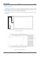
Application Note [Page 9] Figure 2.4 PCB Design 2.5 RF Design 2.5.1 On-board PCB Antenna Design The main board PCB should be over 16mm far away from other metal components. Copper, route, closing to metal element is not allowed if the structure needed. P1 to P8 should connect to ground with copper. PCB part below antenna could be hollowed up.
Application Note [Page 10] Figure 2.5 Minimum PCB Clearance Area In order to reduce the influence from metal components to PCB antenna and wireless signal, it is better to mount EMW3239 on four parts. Figure 2.6 Position of the Module 2.5.2 External Antenna Size of external antenna is shown in figure 2.7.
Application Note [Page 11] connectors of antenna. Figure 2.7 Size of External Antenna 2.6 ESD Design ESD level of the module: Human body model (HBM) is 2000V, charged device model (CDM) is 500V. Position of ESD protected components should be reserved if the products require higher ESD requirement such as pins connect to USB and SD-card. EMI should be aware when the module operated by connecting external wire. Using shielding wire or reserving common mode choke could avoid EMI.
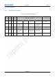
Application Note [Page 12] 3. Downloading Firmware and Storage Test Method 3.1 Preparations Table 3.1Device List Device Quantity PC 1 Tools of downloading firmware 1 EMW3239 1 Micro USB 1 Downloading Software 1 Testing Software 1 Download website is shown in table 3.2. Table 3.2Download Websites Name Function Websites FWUpdate Download http://pan.baidu.com/s/1kVEwnNh MicoQcAutoCheck4.0 Test http://pan.baidu.com/s/1kVEwnNh CP210x_VCP_Windows USB Drever http://www.silabs.
Application Note [Page 13] Figure 3.1Switch Set Up Decompress file ‘CP210X_VCP_WINDOWS.ZIP’. 32 or 64 is based on the computer operating system. It could be checked from device manager after installing. 3.3 System Connection Module connects to develop board of EMW3031 with USB. Green light D1 on the develop board enable when connecting. Figure 3.2Power Light 3.4 Serial Port Selection Find COM number of develop board connect to PC, such as COM4 in figure 3.3.
Application Note [Page 14] Figure 3.4 Install J-Flash ‘JFlash V6.00’ would be found after installing. Figure 3.5 J-Flash signature 3.6 J-Flash Set Up Use ‘ALT+F7’ or open ‘Options’ then click ‘project settings’. Select ‘SWD’ in Target Interface, ‘ST STM32F412RG’ in MCU, ‘Start application’ in Production. Figure 3.
Application Note Figure 3.7 MCU Set Up Figure 3.8 Production Set Up Click ‘OK’ after set up. There would be no more set up in following downloading if save the set up. 3.7 Testing 3.7.1 Environment Set Up Turn on 5 routers that randomly located around test module in a range of 2 to 5 meters.
Application Note [Page 16] Figure 3.9 Position of Routers 3.8 Important Statement MXCHIP has a duty to make sure there is no quality problem when sell the module to customers. Customers have the rights to ask MXCHIP to exchange goods if the product has quality problem. If the customer find the problem after welding the module on board without testing at the beginning, MXCHIP is only responsible for the compensation of the module part.
Application Note [Page 17] 4. SMT 4.1 Stencils Stencils thickness is suggested as 0.12mm (0.1~0.15mm) with Laser grinding. Recommended solder paste: No lead SAC305. Stencils size is shown in figure 4.1, pad holes extend 0.15mm in order to improving solder wicking. If there is no AOI testing, check module by eye is available to reduce the Pseudo Soldering. Figure 4.1 Stencils size 4.
Application Note [Page 18] 5. Mass Production Test and Product Update Customers should consider not only the function of product but also the testing method in mass production and update firmware on the product. 5.1 Module Test In order to avoid inferior module and make sure the correct of downloading firmware, MXCHIP strongly suggests product testing before produce. Fully test is required after producing. 5.1.
Application Note 6. Technical Support For consultation or purchase the product, please contact Mxchip during working hours: From Monday to Friday, morning 9:00~12:00, afternoon 13:00~18:00 Telephone: +86-21-52655026 Contact address: 9th Floor, No.5, Lane2145 JinshaJiang Road Putuo District, ShangHai. Postcode:200333 Email: sales@mxchip.
Application Note [Page 20] 7. FCC Statement When this modular approved transmitter is integrated into a final host device, and the FCC ID is not visible from the outside, than the host device must be labeled with an auxiliary label stating “Contains FCC ID: P53-EMW3239”. Following statement shall be placed on the final host device: “This device complies with part 15 of the FCC Rules.