
User's Manual
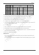
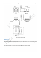
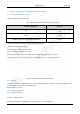
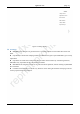
Table Of Contents

[Page 9]
EMW3166
Pins
Name
Type
I/O level
Functions
Note
37
PB0
I/O
FT
GPIO
ADC1_8
×(STATUS)
38
PA4
I/O
TC
GPIO
ADC1_4
√
39
VDD
S
-
3.3V
×
40
VDD
S
-
3.3V
×
41
ANT
-
-
ANT
×
Notes:
1. PIN10, PIN39, PIN40 need connect to VDD 3V3 power and PIN20, PIN21 connects to GND.
2. PIN8 and PIN12 are used for secondary burning, ATE and QC auto detection.
3. PIN29 and PIN30 are used as serial communication port for application.
4. “S” indicates “power supply”, “I” indicates “input pin”, “I/O” indicates “input/output pin”.
5. “FT” indicates the maximum tolerance input voltage is 5V. The maximum tolerance voltage could not be over
VCC when configured as analog I/O or RTC.
6. TC=standard 3.6V I/O.
7. PIN4~7 could not be used as the other functions except for the SPI1 interface of on-board flash.
8. Take SWD (PIN25, PIN26) as the replacement of JTAG to debug or download firmware.
9. “√” indicates the pin which could be used for customized applications, while “×” could not be used besides two
groups “serial” and one group “SPI”.
10. Please refer to MXCHIP for more support.
Important Note:
If developers build an application based on MICO system, they can define or modify the function for
every pin on EMW3166.
The pin arrangement of the firmware MXCHIP developed could take the Application Note as a reference.