
Data Sheet


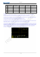


Table Of Contents

Datasheet
7 / 21
Pin
FUNCTION1
FUNCTION2
FUNCTION3
FUNCTION4
FUNCTION5
14
MICO_GPIO_1
MICO_PWM1
SWD_CLK
15
MICO_GPIO_10
MICO_I2C1_CLK
MICO_UART0_RXD
MICO_SPI1_CLK
16
MICO_GPIO_9
MICO_I2C1_SDA
MICO_UART0_TXD
MICO_PWM1
MICO_SPI1_MOSI
17
MICO_GPIO_19
BOOT
Description:
(1) The GPIO19 pin defaults to BOOT; the GPIO23 pin is used by EASYLINK; the PIN11/12 pin is used for debugging log
information output. Please try not to use the hardware design. Please contact our engineers for confirmation.
(2) The PIN11 pin can't be pulled low and then powered on. The PWM3 power-on must be in the “L” state, and the module has made
10k resistor pull-down inside. Please pay special attention when designing the circuit.
(3) CHIP_EN is the enable pin. Pulling low and then pulling high will generate a chip reset.
(4) CHIP_EN, PIN11/12 has 10k pull-up inside; except PWM corresponding to SWD and UART1 (Debug) pin, other PWM1, PWM3,
PWM4, PWM5, PWM6 have 10k pull-down inside; please allocate relevant peripheral devices reasonably.
(5) Other pins that are not used can be left floating. It should be noted that the IO port is a floating state at startup. This is the case from
the beginning of the ROM code. It is also necessary to go to the boot code at the earliest. Up and down, and the time elapsed in it will
be affected by the flash, so if the module needs to be at the level determined by the module at startup, it needs to externally pull at least
100k resistor to externally pull up to stabilize the level. If the figure below shows the level of the IO port that is configured to be
normally low after the module is started, the floating state is pulled up by the external 100K resistor.