
Data Sheet


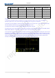


Table Of Contents

Datasheet
5 / 21
This device complies with part 15 of the FCC Rules. Operation is subject to the following two conditions: (1) This
device may not cause harmful interference, and (2) this device must accept any interference received, including
interference that may cause undesired operation.
Pin Arrangement
EMW3092 adopts a through-hole and SMT package design. The stamp hole package design is convenient for
customer debugging, easy to disassemble and easy to use for SMT. The left and right pads are 1.2x1.6mm and the
lower pads are 1.2x0.8mm. The motherboard pad is recommended to expand 0.1mm.Solder mask opening and pad
size are the same. SMT recommends stencil thickness 0.12mm-0.14mm.
Figure 2 Module Picture
Figure 3 DIP Package Size