
Data Sheet


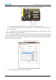


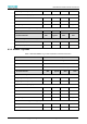
Table Of Contents
- Abstract
- 1. Introduction
- 2. Characteristics
- 3. Pin Definition
- 4. System memory Space
- 5. ATE(RF Test Mode)
- 5.1. Wi-Fi ATE Command
- 5.1.1. Start MP mode
- 5.1.2. Stop MP mode
- 5.1.3. Set Tx rate
- 5.1.4. Set operational channel
- 5.1.5. Set operational bandwidth
- 5.1.6. Set Tx power
- 5.1.7. Set antenna for Tx
- 5.1.8. Set antenna for Rx
- 5.1.9. Start air Rx mode
- 5.1.10. Start continuous Tx mode
- 5.1.11. Query air Rx statistics
- 5.1.12. Reset air Tx/Rx statistics
- 5.2. Bluetooth ATE Command(TBD)
- 5.3. Example Command
- 5.1. Wi-Fi ATE Command
- 6. Flash Programming
- 7. Electrical Parameters
- 8. RF Parameter
- 9. Antenna Information
- 10. Dimensions and Production Guidance
- 11. Production Guidelines
- 12. FCC and IC Information
- 12.1. FCC Warning
- 12.2. IC warning
- 12.3. Trace antenna designs
- 12.4. RF exposure considerations
- 12.5. Antennas
- 12.6. Label and compliance information
- 12.7. Information on test modes and additional testing requirements5
- 12.8. Additional testing, Part 15 Subpart B disclaimer
- 12.9. The module is limited to OEM installation ONLY.
- 12.10. The OEM integrator is responsible for ensuring that the end-user has no manual instructions to remove or install module.
- 12.11. The module is limited to installation in mobile or fixed applications
- 13. Packaging and Label Information
- 14. Sales and Technical Support Information

EMC3380 Series Wireless Module Data Manual
Copyright of Shanghai MXCHIP Information Technology Co., Ltd.
34
Table 13 RF consumption under 3.3V
Operation Mode
Current
Unit
2.4G
5G
1T-MCS7/BW40M (15dBm)
206
286
mA
1T-MCS7/BW40M (18dBm@2.4G, 17dBm@5G)
247
310
1T-MCS7/BW20M (15dBm)
204
286
1T-MCS7/BW20M (18dBm)
248
308
1T-Legacy_OFDM54M (16dBm)
214
296
1T-Legacy_OFDM54M (19dBm@2.4 18dBm@5G)
262
323
1T_CCK11M (18dBm)
257
1T_CCK11M (21dBm)
312
1R-Idle/BW40
52
53
1R-MCS7/BW40M (Pin= -60dBm)
61
64
1R-MCS7/BW20M (Pin= -60dBm)
62
63
1R-Legacy_OFDM54M (Pin= -60dBm)
61
62
1R-CCK11M (Pin= -60dBm)
52
RF Standby
24
23
RF Disable
24
23
Digital IO DC characteristic
The electrical characteristics of the module's digital IO port are described in Table 13 under 3.3V power
supply.
Table 14 operation parameter(3.3V):Digital IO DC characteristic
Sym
bol
Note
Conditions
Specification
Min.
Typical
Max.
U
nit
V
IH
Input-High Voltage
LVTTL
2.0
-
-
V
V
IL
Input-Low Voltage
LVTTL
-
-
0.8
V
V
OH
Output-High Voltage
LVTTL
9.58
9.59
13.43
V
V
OL
Output-Low Voltage
LVTTL
0.4
V
I
IL
Input-Leakage Current
V
IN
= 3.3V/0V
-10
±1
10
𝝻A