
Data Sheet


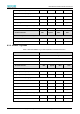
Table Of Contents
- Abstract
- 1. Introduction
- 2. Characteristics
- 3. Pin Definition
- 4. System memory Space
- 5. ATE(RF Test Mode)
- 5.1. Wi-Fi ATE Command
- 5.1.1. Start MP mode
- 5.1.2. Stop MP mode
- 5.1.3. Set Tx rate
- 5.1.4. Set operational channel
- 5.1.5. Set operational bandwidth
- 5.1.6. Set Tx power
- 5.1.7. Set antenna for Tx
- 5.1.8. Set antenna for Rx
- 5.1.9. Start air Rx mode
- 5.1.10. Start continuous Tx mode
- 5.1.11. Query air Rx statistics
- 5.1.12. Reset air Tx/Rx statistics
- 5.2. Bluetooth ATE Command(TBD)
- 5.3. Example Command
- 5.1. Wi-Fi ATE Command
- 6. Flash Programming
- 7. Electrical Parameters
- 8. RF Parameter
- 9. Antenna Information
- 10. Dimensions and Production Guidance
- 11. Production Guidelines
- 12. FCC and IC Information
- 12.1. FCC Warning
- 12.2. IC warning
- 12.3. Trace antenna designs
- 12.4. RF exposure considerations
- 12.5. Antennas
- 12.6. Label and compliance information
- 12.7. Information on test modes and additional testing requirements5
- 12.8. Additional testing, Part 15 Subpart B disclaimer
- 12.9. The module is limited to OEM installation ONLY.
- 12.10. The OEM integrator is responsible for ensuring that the end-user has no manual instructions to remove or install module.
- 12.11. The module is limited to installation in mobile or fixed applications
- 13. Packaging and Label Information
- 14. Sales and Technical Support Information

EMC3380 Series Wireless Module Data Manual
Copyright of Shanghai MXCHIP Information Technology Co., Ltd.
32
Electrical Parameters
Working Condition
When the input voltage is lower than the lowest rated voltage, the operation will be unstable. This
should be noted in power supply design.
Table 9 Input Voltage Range
Symbol
Description
Condition
Detail
Minimum
Typical
Maximum
Unit
V
DD
Power Voltage
2.7
3.3
3.6
V
Absolute Maximum Parameter
Modules operating outside the absolute maximum ratings may cause permanent damage. At the same
time, long-term exposure to the maximum rating conditions will affect the reliability of the module.
Table 10 Absolute maximum parameter: voltage
Symbol
Ratings
Min
Max
Uni
t
V
DD
–V
SS
Voltage
–0.3
3.6
V
V
IN
Input voltage on any other pin
V
SS
−0.3
V
DD
+0.3
V
Operation Voltage and Current
Table 11 operating parameter: voltage and current
Symbol
Note
Specification
Min.
Typic
al
Ma
x.
Unit
V
DD
Voltage
3.0
3.3
3.6
V
I
VDD
3.3V Rating Current (with internal regulator and
integrated CMOS PA)
450
mA
Table 12 Average power consumption under 3.3V
Operation Mode
Conditions
Aver
age
Current
Un
it
Power
Mode
Scenario
Deepsleep
Deepsleep
RTC timer
7~8
𝝻
A