
Data Sheet
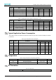
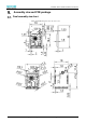
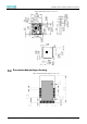
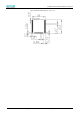
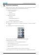
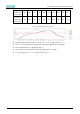
Table Of Contents
- Abstract
- 1. Introduction
- 2. Characteristic
- 3. Pin Definition
- 4. System memory space
- 5. ATE(RF Test Mode)
- 5.1. ATE Command
- 5.1.1. Start MP mode
- 5.1.2. Stop MP mode
- 5.1.3. Set Tx rate
- 5.1.4. Set operational channel
- 5.1.5. Set operational bandwidth
- 5.1.6. Set Tx power
- 5.1.7. Set antenna for Tx
- 5.1.8. Set antenna for Rx
- 5.1.9. Start air Rx mode
- 5.1.10. Start continuous Tx mode
- 5.1.11. Query air Rx statistics
- 5.1.12. Reset air Tx/Rx statistics
- 5.2. Example Command
- 5.1. ATE Command
- 6. Flash Programing
- 7. Electrical parameters
- 8. Antenna Information
- 9. Assembly size and PCB package
- 10. Production Guidelines
- 11. FCC and IC Information
- 11.1. FCC Warning
- 11.2. IC warning
- 11.3. Trace antenna designs
- 11.4. RF exposure considerations
- 11.5. Antennas
- 11.6. Label and compliance information
- 11.7. Information on test modes and additional testing requirements5
- 11.8. Additional testing, Part 15 Subpart B disclaimer
- 11.9. The module is limited to OEM installation ONLY.
- 11.10. The OEM integrator is responsible for ensuring that the end-user has no manual instructions to remove or install module.
- 11.11. The module is limited to installation in mobile or fixed applications
- 12. Package and Label
- Appendix 1: Sales and Technical Support Information

EMC328x Series Wireless Module Data Manual
Copyright of Shanghai MXCHIP Information Technology Co., Ltd.
24
Symbol
Note
Conditions
Specification
Min.
Typical
Max.
Unit
V
IL
Input-Low Voltage
LVTTL
-
-
0.8
V
V
OH
Output-High Voltage
LVTTL
9.58
9.59
13.43
V
V
OL
Output-Low Voltage
LVTTL
0.4
V
I
IL
Input-Leakage Current
V
IN
= 3.3V/0V
-10
±1
10
𝝻A
Table 11 Operating Parameters: Digital IO DC Characteristics(1.8V)
Symbol
Note
Conditions
Specification
Min.
Typical
Max.
Unit
V
IH
Input-High Voltage
CMOS
0.65 x V
DD
-
-
V
V
IL
Input-Low Voltage
CMOS
-
-
0.35 x V
DD
V
V
OH
Output-High Voltage
CMOS
V
DD
-0.45
-
-
V
V
OL
Output-Low Voltage
CMOS
0.45
V
I
IL
Input-Leakage Current
V
IN
= 1.8V/0V
-10
±1
10
𝝻A
Typical Application Power Consumption
The module current test environment is based on VDD=3.3V, the CPU is clocked at 52MHz, and UART1
is turned on.
Table 12 Typical Application Power Consumption
Symbol
Note
Conditions
Specification
Min.
Average
Max.
Unit
I
VDD
KM0, KM4
KM0&KM4 run
TBD
TBD
TBD
mA
I
VDD
Only MCU
Kernel sleep, disable Wi-Fi
TBD
TBD
TBD
mA
I
VDD
MCU&RF
Station mode, no data transmitting
TBD
TBD
TBD
mA
I
VDD
MCU&RF
Station mode, enter power save mode
TBD
TBD
TBD
mA
I
VDD
MCU&RF
Station mode, send UDP packet per 100ms
TBD
TBD
TBD
mA
I
VDD
MCU&RF
Soft AP mode, beacon interval = 100ms
TBD
TBD
TBD
mA
I
VDD
MCU&RF
Monitor mode
TBD 4
TBD
TBD
mA
Temperature
Table 13 Storage Temperature and Operating Temperature
Symbol
Ratings
Max
Unit
T
STG
Storage temperature
–55 to +125
℃
T
A
Working temperature
-20 to +85
℃
RF Parameters
Table 14 RF Parameters
Item
Specification