
Data Sheet
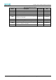
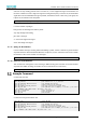
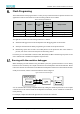
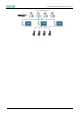
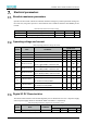
Table Of Contents
- Abstract
- 1. Introduction
- 2. Characteristic
- 3. Pin Definition
- 4. System memory space
- 5. ATE(RF Test Mode)
- 5.1. ATE Command
- 5.1.1. Start MP mode
- 5.1.2. Stop MP mode
- 5.1.3. Set Tx rate
- 5.1.4. Set operational channel
- 5.1.5. Set operational bandwidth
- 5.1.6. Set Tx power
- 5.1.7. Set antenna for Tx
- 5.1.8. Set antenna for Rx
- 5.1.9. Start air Rx mode
- 5.1.10. Start continuous Tx mode
- 5.1.11. Query air Rx statistics
- 5.1.12. Reset air Tx/Rx statistics
- 5.2. Example Command
- 5.1. ATE Command
- 6. Flash Programing
- 7. Electrical parameters
- 8. Antenna Information
- 9. Assembly size and PCB package
- 10. Production Guidelines
- 11. FCC and IC Information
- 11.1. FCC Warning
- 11.2. IC warning
- 11.3. Trace antenna designs
- 11.4. RF exposure considerations
- 11.5. Antennas
- 11.6. Label and compliance information
- 11.7. Information on test modes and additional testing requirements5
- 11.8. Additional testing, Part 15 Subpart B disclaimer
- 11.9. The module is limited to OEM installation ONLY.
- 11.10. The OEM integrator is responsible for ensuring that the end-user has no manual instructions to remove or install module.
- 11.11. The module is limited to installation in mobile or fixed applications
- 12. Package and Label
- Appendix 1: Sales and Technical Support Information

EMC328x Series Wireless Module Data Manual
Copyright of Shanghai MXCHIP Information Technology Co., Ltd.
23
Electrical parameters
Absolute maximum parameters
Operation of the module outside of its absolute maximum ratings may result in permanent damage. At
the same time, long-term exposure to the maximum rated conditions will affect the reliability of the
module.
Table 8 Absolute Maximum Parameter: Voltage
Symbol
Ratings
Min
Max
Unit
V
DD
–V
SS
Voltage
–0.3
3.6
V
V
IN
Input voltage on any other pin
V
SS
−0.3
V
DD
+0.3
V
Operating voltage and current
Table 9 Operating parameters: voltage and current
Symbol
Note
Conditions
Specification
Min.
Typical
Max.
Unit
V
DD
Voltage
1.62
1.8, 3.3
3.6
V
I
VDD
Current
Run mode
(1)
450
mA
I
VDD
RF Idle
Run mode
(1)
, Wi-Fi off, BT off
9.58
9.59
13.43
mA
I
VDD
Wi-Fi RX Current
Run mode
(1)
, Wi-Fi on, BT off
TBD
mA
I
VDD
Wi-Fi TX Current
Run mode
(1)
, Wi-Fi on, BT off,
802.11b 11M@18dBm, continuous send
TBD
mA
I
VDD
Wi-Fi TX Current
Run mode
(1)
, Wi-Fi on, BT off,
802.11g 54M@15dBm, continuous send
TBD
mA
I
VDD
Wi-Fi TX Current
Run mode(1), Wi-Fi on, BT off,
802.11n MCS7@13dBm, continuous send
TBD
mA
I
VDD
BT RX Current
Run mode
(1)
, Wi-Fi off, BT on
TBD
mA
I
VDD
BT TX Current
Run mode(1), Wi-Fi off, BT on,
BLE continuous send @10dBm
TBD
mA
I
VDD
BT TX Current
Run mode(1), Wi-Fi off, BT on,
BLE continuous send @4dBm
TBD
mA
I
VDD
Standby
V
DD
=3.3V
uA
Run mode: V
DD
=3.3V, KM0@20MHz, KM4@200MHz, UART_LOG enable
Digital IO DC Characteristics
The electrical characteristics of the module digital IO port are divided into two cases: 1.8V power supply
and 3.3V power supply, which are described in Table 10 and Table 11, respectively.
Table 10 Operating Parameters:Digital IO DC Characteristics(3.3V)
Symbol
Note
Conditions
Specification
Min.
Typical
Max.
Unit
V
IH
Input-High Voltage
LVTTL
2.0
-
-
V