
Data Sheet

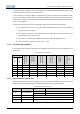
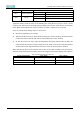
Table Of Contents
- Abstract
- 1. Introduction
- 2. Characteristic
- 3. Pin Definition
- 4. System memory space
- 5. ATE(RF Test Mode)
- 5.1. ATE Command
- 5.1.1. Start MP mode
- 5.1.2. Stop MP mode
- 5.1.3. Set Tx rate
- 5.1.4. Set operational channel
- 5.1.5. Set operational bandwidth
- 5.1.6. Set Tx power
- 5.1.7. Set antenna for Tx
- 5.1.8. Set antenna for Rx
- 5.1.9. Start air Rx mode
- 5.1.10. Start continuous Tx mode
- 5.1.11. Query air Rx statistics
- 5.1.12. Reset air Tx/Rx statistics
- 5.2. Example Command
- 5.1. ATE Command
- 6. Flash Programing
- 7. Electrical parameters
- 8. Antenna Information
- 9. Assembly size and PCB package
- 10. Production Guidelines
- 11. FCC and IC Information
- 11.1. FCC Warning
- 11.2. IC warning
- 11.3. Trace antenna designs
- 11.4. RF exposure considerations
- 11.5. Antennas
- 11.6. Label and compliance information
- 11.7. Information on test modes and additional testing requirements5
- 11.8. Additional testing, Part 15 Subpart B disclaimer
- 11.9. The module is limited to OEM installation ONLY.
- 11.10. The OEM integrator is responsible for ensuring that the end-user has no manual instructions to remove or install module.
- 11.11. The module is limited to installation in mobile or fixed applications
- 12. Package and Label
- Appendix 1: Sales and Technical Support Information

EMC328x Series Wireless Module Data Manual
Copyright of Shanghai MXCHIP Information Technology Co., Ltd.
10
(1). Special function capture pin, the module will detect the status of these pins when starting up and
enter special functions, please refer to chapter 3.2.3
(2). The default state of the pin. When the Reset button is pressed, all GPIO ports will remain in their
previous state. When the Reset button is released, the GPIO state returns to the state described in
"Default State" in Table 1, where EfusePullCtrlx indicates that the default state of the pin is the status bits
in eFuse are determined.
(3). The time from system power-up to GPIO power supply can be divided into three phases:
⚫ The supply voltage rises to 1.5V and the internal AON_LDO voltage rises to 0.5V. Determined
by 3.3V/1.8V power-on time
⚫ The internal analog circuit of the chip needs 6ms to supply power to the Reset button, and
then the digital circuit starts to work.
⚫ After 300us~1.5ms, the general GPIO is powered, the default level will take effect.
⚫ Phase 2 and Phase 3 require a total of 6.3ms ~ 7.5ms
3.2.2. Low Power Pin Definition
Low-power pins can wake the module from the Deep Sleep state and are located on the keyboard scan
function pin.
Table 2 Low Power Pin Definition
3.2.3. Special Function Capture Pins
The status of these pins is detected during power-up of the module, allowing access to certain special
modes and functions. These features are hardware determined and cannot be modified.
Table 3 Special function capture pin
Pin Name
Trap Function
State
Description
PA7
UART_DOWNLOAD
High(Default)
Normal boot application
Low
Boot ROM code and enter flash download mode
PA12
ICFG0
Test mode, if not entering test mode, can be ignored
PA13
ICFG1
Test mode, if not entering test mode, can be ignored
PA14
ICFG2
Test mode, if not entering test mode, can be ignored
Pin Number
Name (function
after reset)
Function 28
(Ext32K)
Function 29
(key scan row)
Function 30
(key scan col)
Function 31
(wakeup)
PX_FUNC_DEFA
ULT
EMC3280
EMC3285
14
9
PA12
KEY_ROW0
LGPIO0
GPIOC_LP0
15
8
PA13
KEY_ROW1
LGPIO1
GPIOC_LP1
19
6
PA14
RTC_OUT
KEY_ROW2
LGPIO2
GPIOC_LP2
23
7
PA15
RTC EXT_32K
KEY_ROW3
KEY_COL6
LGPIO3
GPIOC_LP3
10
11
PA25
KEY_COL1
LGPIO2
GPIOC_LP10
9
12
PA26
KEY_COL0
LGPIO3
GPIOC_LP11