
Data Sheet
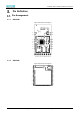

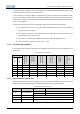
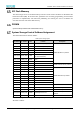
Table Of Contents
- Abstract
- 1. Introduction
- 2. Characteristic
- 3. Pin Definition
- 4. System memory space
- 5. ATE(RF Test Mode)
- 5.1. ATE Command
- 5.1.1. Start MP mode
- 5.1.2. Stop MP mode
- 5.1.3. Set Tx rate
- 5.1.4. Set operational channel
- 5.1.5. Set operational bandwidth
- 5.1.6. Set Tx power
- 5.1.7. Set antenna for Tx
- 5.1.8. Set antenna for Rx
- 5.1.9. Start air Rx mode
- 5.1.10. Start continuous Tx mode
- 5.1.11. Query air Rx statistics
- 5.1.12. Reset air Tx/Rx statistics
- 5.2. Example Command
- 5.1. ATE Command
- 6. Flash Programing
- 7. Electrical parameters
- 8. Antenna Information
- 9. Assembly size and PCB package
- 10. Production Guidelines
- 11. FCC and IC Information
- 11.1. FCC Warning
- 11.2. IC warning
- 11.3. Trace antenna designs
- 11.4. RF exposure considerations
- 11.5. Antennas
- 11.6. Label and compliance information
- 11.7. Information on test modes and additional testing requirements5
- 11.8. Additional testing, Part 15 Subpart B disclaimer
- 11.9. The module is limited to OEM installation ONLY.
- 11.10. The OEM integrator is responsible for ensuring that the end-user has no manual instructions to remove or install module.
- 11.11. The module is limited to installation in mobile or fixed applications
- 12. Package and Label
- Appendix 1: Sales and Technical Support Information

EMC328x Series Wireless Module Data Manual
Copyright of Shanghai MXCHIP Information Technology Co., Ltd.
6
⚫ I2C
▪ Two-wire I2C serial interface consisting of data line (SDA) and clock line (SCL)
▪ Supports one I2C interface, supports two standard modes with a maximum rate of 100Kbps and
a high-speed mode of 400Kbps, and supports clock stretching.
▪ Support I2C master or slave device
▪ Support 7-bit or 10-bit address addressing and support mixed transmission
▪ Receive and send buffers with 16 words depth
▪ Support DMA for data transmission and reception
▪ Support bus arbitration mechanism to realize communication capability of multi-master devices
▪ Wake-up from device address match for low power consumption
▪ Software configurable parameters: SDA hold time, slave address, etc.
▪ Programmable SDA and SCL signal digital filters for filtering noise on signal lines
Timer
⚫ Basic Timer(HS_TIM0 ~ HS_TIM3,LP_TIM0 ~ LP_TIM3)
▪ Clock source: 32KHz, accuracy: 32 bits, counting mode: counting up
▪ Support interrupt trigger, sleep mode wake-up
⚫ PWM Timer(HS_TIM5 ,LP_TIM5)
▪ Channel: HS_TIM5 x 8 , LP_TIM5 x 4
▪ Clock source: XTAL, accuracy: 16 bits, counting mode: increment counting, frequency division: 8
bits
▪ 1 x input capture pin
▪ LP_TIM5 can work in low power mode
⚫ Real Time Clock (RTC)
▪ Independent BCD counter
▪ Day/hour/minute/second, 12 or 24 hour format clock
▪ Software programmable clock compensation
▪ An alarm that can be triggered by any combination of time domains and generate an interrupt
▪ Digital calibration circuit
▪ Register write protection
Human-Computer Interaction Interface
⚫ Matrix keyboard
▪ 6 IO ports, up to 4 x 2, 3 x 3 matrix keyboard scanning
▪ Number of configurable keyboard rows and columns
▪ Configurable scan clock, scan interval and release time