
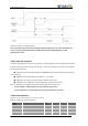
Specifications

L506 Hardware Design
Copyright© Shanghai Mobiletek Communication Ltd 49
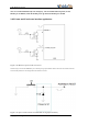
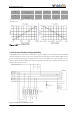
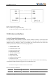
Figure 3-26 I2C reference design
Note: 1. L506 I2C only support host mode.
2. Only special software version support inquire the I2C.
3.16 Antenna interface
3.16.1 RF signal PCB layout guide
L506 provides RF antenna interface. Customer’s antenna should be located in the host board and
connected to module’s antenna pad through micro-strip line or other types of RF trace and the trace
impedance must be controlled in 50Ω. we recommends that the total insertion loss between the
antenna pad and antenna should meet the following requirements:
● GSM900/GSM850<0.5dB
● DCS1800/PCS1900 <0.9dB
● WCDMA 2100/1900<0.9dB
● WCDMA 900/850<0.5 dB
● TDSCDMA 900/850<0.5dB
● CDMA BC0<0.5dB
● LTE (F<1GHz) <0.5dB
● LTE (1GHz<F<2GHz) <0.9dB
● LTE (2GHz<F) <1.2dB
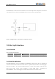
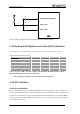
To facilitate the antenna tuning and certification test, a RF connector and an antenna matching
circuitshould be added. The following figure is the recommended circuit.
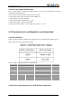
The antenna feed point is defined as shown in below table:
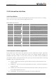
Table 3-25 antenna pin definition
Pin No.
Signal
I/O Typ.
Description
82
MAIN_ANT
AI/AO
Module main antenna