
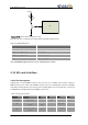
Specifications

L506 Hardware Design
Copyright© Shanghai Mobiletek Communication Ltd 47
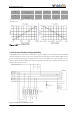
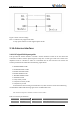
3.12.3 SD card signal PCB line rules
Due to the SD signal is the high-speed digital interface, so it’s layout rules should be in accordance
with the high speed digital rules.
1.Protect other sensitive signals/circuits from SDC corruption.
2. Protect SDC signals from noisy signals (clocks, SMPS, etc.).
3. 50 Ω nominal, ±10% trace impedance.
4. CLK to DATA/CMD length matching < 1 mm.
5. Total routing length < 50 mm recommended.
6. Spacing to all other signals = 2x line width.6 Bus capacitance < 15 pF.
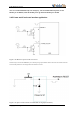
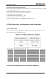
3.13 System boot configuration and download
3.13.1 Pin definition
L506 can configure BOOT_CONFIG (Boot Configuration) pin to Configuration module power-on
mode and the forced entry USB download mode.
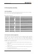
Table 3-23 Boot configurationand force USB download
Pin No.
Net name
Function description
note
85
BOOT_CFG0
Pull up this pin change boot
configurationregister value
87
BOOT_CFG1
Pull up this pin change boot
configurationregister value
84
COEX2(Syste
m on)
FOCE_USB_BOOT(
before system
on)
Pull up this pin change boot
configurationregister value
Multiplex
pin
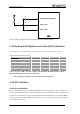
3.13.2 Boot configuration and force USB interface application