
Specifications
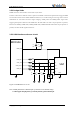

L506 Hardware Design
Copyright© Shanghai Mobiletek Communication Ltd 31
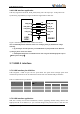
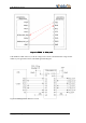
effective the emission spectrum and receiving sensitivity, etc. So the power supply part design is very
important, when you design this part you should notes below contents: 1. DC DC switch power should
place away from the antenna and other sensitivity circuit; 2. Consider the voltage drop and the module
current requirement, the layout line should better above 100mil. If conditions allow should add a
power shape plane.
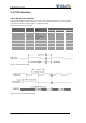
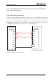
3.5 USIM interface
3.5.1 Pin definition
The L506 integrated a ISO 7816-2 standard USIM port, and the module can automatic identify the
voltage demo according the USIM to allow the mobile equipment toattach to the network. Both 1.8V
and 3.0V SIM Cards are supported.
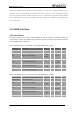
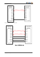
Table 3-9USIM Electronic characteristic in 1.8V mode (USIM_VDD =1.8V)
Symbol
Parameter
Min.
Typ.
Max.
Unit
USIM_VDD
LDO power output
1.75
1.8
1.95
V
VIH
High-level input voltage
0.65·USI
M_VDD
-
USIM_V
DD +0.3
V
VIL
Low-level input voltage
-0.3
0
0.35·USI
M_VDD
V
VOH
High-level output voltage
USIM_V
DD -0.45
--
USIM_V
DD
V
VOL
Low-level output voltage
0
0
0.45
V
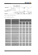
Table 3-10: USIM Electronic characteristic 3.0V mode (USIM_VDD =2.85V)
Symbol
Parameter
Min.
Typ.
Max.
Unit
USIM_VDD
LDO power output
2.75
2.85
3.0
V
VIH
High-level input voltage
0.65*USI
M_VDD
-
USIM_V
DD +0.3
V
VIL
Low-level input voltage
-0.3
0
0.25·USI
M_VDD
V
VOH
High-level output voltage
USIM_V
DD -0.45
-
USIM_V
DD
V
VOL
Low-level output voltage
0
0
0.45
V