
Specifications


L506 Hardware Design
Copyright© Shanghai Mobiletek Communication Ltd 30
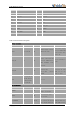
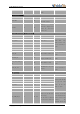
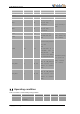
NO.
Manufacturer
Part Number
Power
Package
1
On semi
MMSZ5231BT1G
500mW
SOD123
2
Prisemi
PZ3D4V2H
500mW
SOD123
3
Vishay
MMSZ4689-V
500mW
SOD123
4
Crownpo
CDZ55C5V1SM
500mW
0805
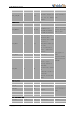
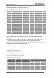
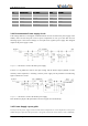
3.4.4 Recommended Power supply circuit
If the voltage difference is not big,We recommend DCDC or LDO is used for the power supply of the
module, make sure that the peak current of power components can rise up to more than 2A. The
following figure is the reference design of +5V input linear regulator power supply. The designed
output for the power supply is 3.8V.
Figure 3-4 Reference circuit of the LDO power supply
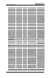
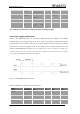
If there is a big difference between the input voltage and the desired output (VBAT) or better
efficiency ismore important, a switching converter power supply will be preferable. The following
figure is thereference circuit.
Figure 3-5 Reference circuit of the DCDC power supply
Note: DCDC may deprave RF performance because of ripple current intrinsically.
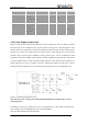
3.4.5 Power Supply Layout guide
The layout of the power supply section and the related components is of vital importance in the power
module design. If processes this part layout is not good, will lead to various effects, such as bad EMC,