
Specifications

L506 Hardware Design
Copyright© Shanghai Mobiletek Communication Ltd 27
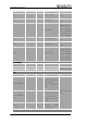
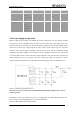
3.3 Digital I/O characteristics
Table 3-5 1.8V Digital I/O characteristics
Parameter
Description
Min.
Typ.
Max.
Unit
VIH
High level input voltage
0.7*VDD_PX
VDD_PX
VDD_PX+0.3
V
VIL
Low level input voltage
-0.3
0
0.2* VDD_PX
V
VOH
High level output voltage
VDD_PX-0.45
-
VDD_PX
V
VOL
Low level output voltage
0
0
0.45
V
IOH
High-level output current
(nopull down resistor)
-
2
-
mA
IOL
Low-level output current
(no pullup resistor)
-
-2
-
mA
IIH
Input high leakage
current (no
pull down resistor)
-
-
1
uA
IIL
Input low leakage current
(nopull up resistor)
-1
-
-
uA
*Note: 1. These parameters are for digital interface pins, such as SPI, WIFI SDIO, GPIOs
(NETLIGHT,
FLIGHTMODE, STATUS, USIM_DET, SD1_DET), I2C, UART, PCM, COEXn, BOOT_CFGn.
2. L506 TF-card signal(SD_DATA0~SD_DATA3,SD_CLK,SD_CMD),USIM card
signal(USIM_CLK,USIM_DATA,USIM_RST) support dual-voltage(1.8V and 3.0V)mode, and the
DC character show in corresponding function block.
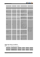
3.4 Power Interface
3.4.1 Power supply pin description
Table 3-6 DC Power Characteristics
Pin No.
Net Name
Description
DC Characteristic(V)
Min.
Typ.
Max.
38,39,62,63
VBAT
Power supply for
the module
3.4
3.8
4.2
1,2,5,10,14,37,40,
41,43,57,58,60,61,
64,65,77,78,80,81
GND
GND
-
-
-