
Specifications

L506 Hardware Design
Copyright© Shanghai Mobiletek Communication Ltd 26
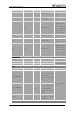
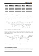
Pin Name
Pin No.
I/O
Description
Content
MAIN _ANT
82
AIO
Main Antenna
Others
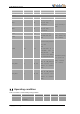
Pin Name
Pin No.
I/O
Description
Content
ADC1
47
AI
Analog conversion
digital input
interface1
If not use keep it
open.
ADC2
46
AI
Analog conversion
digital input
interface2
COEX1
83
I/O
RF synchronizing
between wifi and
LTE.
If not use keep it
open. Normal use
can’t Pullup.
COEX3
86
I/O
COEX2
84#
I/O
Default: RF
synchronizing between
wifi and
LTE.
Optional:Pull up to
1.8V(L506 PIN 15
VDD_1V8)with 10K
resistor force module
in USB download mode
Recommend placing
test points for
debug. Normally
can’t Pullup.
BOOT_CFG0
85
DI, PD
Pull up to 1.8V(L506
PIN 15 VDD_1V8)with
10K resistor force
module in fastboot
mode
BOOT_CFG1
87
DI, PD
Pull up to 1.8V(L506
PIN 15 VDD_1V8)with
10K resistor force
module in fastboot
mode
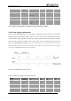
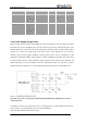
3.2 Operating condition
Table 3-4 module recommendedoperatingcondition
Parameter
Description
Min.
Typ.
Max.
Unit
VBAT
Main power supply for
the module
3.4
3.8
4.2
V