
Specifications

L506 Hardware Design
Copyright© Shanghai Mobiletek Communication Ltd 24
keep it open
GPIO_3/BT_EN
28
I/O
Default: GPIO
Optional: BT_EN pin
for ext bt module
enable
If not use keep it
open
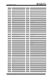
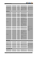
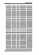
SIMinterface
Pin Name
Pin No.
I/O
Description
Content
USIM_DETECT
53
DI,PU
Input pin as USIM
carddetect pin.
H: USIM is removed
L: USIM is inserted
L506 have internal
pull up. If not use
keep it open.
USIM_DATA
17
I/O
USIM Card data I/O,
which has been
pulled up with a 10KR
resistor to
USIM_VDD in module. Do
not pull
up or pull down in
users’ application
circuit.
All signals of
USIM
interface should
beprotected with
ESD/EMC.
USIM_RESET
18
DO
USIM Reset
USIM_CLK
19
DO
USIM Clock
USIM_VDD
20
PO
USIM Card Power
output, output
Voltage depends on
USIM mode
automatically,and one
is
3.0V±10%, another is
1.8V±10%.
Current is less than
50mA.
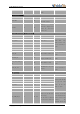
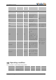
PCM interface
Pin Name
Pin No.
I/O
Description
Content
PCM_CLK
76
DO
PCM data bit clock.
If not use keep it
open.
PCM_SYNC
75
DO
PCM data frame sync
signal.
PCM_IN
74
DI
PCM data input.
PCM_OUT
73
DO
PCM data output.
FULL UART/DEBUG PORT
Pin Name
Pin No.
I/O
Description
Content
RTS
66
DI
DET Request to send.
If not use keep it