
Integration Guide
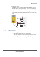
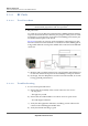
Table Of Contents
- Module Integration Guide
- Preface
- About this Guide
- Introduction
- Manufacturing Process
- Hardware Integration Recommendations
- PCB Layout Rules
- Bring-Up and Testing
- Hardware Test Preparation
- Abbreviations

BRING-UP AND TESTING
FUNCTIONAL VERIFICATION WITHOUT ASSEMBLED MODULE
30 PROPRIETARY MODULE INTEGRATION GUIDE
SEQUANS Communications
5.3.2 RF Path
5.3.2.1 Test Procedure
Important: Those tests should be run or supervised by engineers with RF
measurement preparation and test experience.
• RF path check
To avoid any issue on RF extra path (from the VZM20Q module antenna
output to the board antenna connector), the purpose of this part is to check
its integrity. It corresponds to losses between VZM20Q pin 54 and/or pin
44 and the antenna ports of the board.
Figure 5-3 provides an overview of the equipment configuration for this
test. The connection to the block RF is a connection to the VZM20Q pin 54,
using an RF soldered coaxial probe and RF cable connected to the SMA RF
connector.
Figure 5-3: RF Path Check Setup
a) Measure and record the insertion loss on LTE band 4 and LTE band 13
for the first antenna from pin 54 of the VZM20Q to LTE port antenna
b) By design, the extra RF path loss must be lower than 0.5 dB, to assume
having good RF performances.
5.3.2.2 Troubleshooting
• In case of unexpected RF losses
a) Ensure that the assembly of the coaxial connectors are correct :
- No dry joints.
- The right way round.
b) Ensure that the soldered SMA is not short circuit or open circuit
- Test with digital voltmeter.
c) Verify the RF equipment calibration, including coaxial cable used to
connect to the VZM20Q pin and RF cable
d) Verify that the RF matching is good